
In my last blog, I discussed the conditions that lead to the creation of the boundary scan standard, and I began to describe the internal boundary scan architecture inherent within each IEEE 1149.1 compliant device. As stated, boundary scan is a structural test technology for detecting shorts, opens, and stuck-at faults introduced during the printed circuit board manufacturing process. As boundary scan technology has matured, it is now used for a variety of other applications. In addition to structural test, boundary scan is now used to program parallel flash and Serial Peripheral Interface (SPI) devices, configure Field Programmable Gate Array (FPGA) devices and Complex Programmable Logic Devices (CPLDs), and test the operation of Static Random Access Memory (SRAM), Dynamic Random Access Memory (DRAM), and Double Data Rate (DDR) memory devices.
Before the test for shorts, opens, stuck-at faults are implemented, the boundary architecture of each device must be tested for functionality and the scan chain on the board must be validated. Now, for the manufacturing or test engineer responsible for creating boundary scan test and programming actions, the printed circuit board has already been manufactured and therefore to some extent, the amount of test coverage that can be realized through boundary scan is fixed. Therefore, to maximize the test coverage for a printed circuit board in which boundary scan will be used, it is important that boundary scan design for test (DFT) rules are followed during the device selection and layout stages for the printed circuit board. For more guidelines on boundary scan DFT, please watch my webinar Guidelines for Board Design for Test (DFT) based on Boundary Scan. This webinar covers important steps you should follow to properly design printed circuit boards for boundary scan coverage.
In my previous blog, I described the internal boundary scan architecture and various registers. Boundary scan operations within a device are administered through an embedded controller known as the Test Access Port (TAP). The following TAP signals are used to administer boundary scan operations:
TAP Signals:
Test Data In (TDI) – Represents the serial data shifted into the device’s test or programming logic, is sampled at the rising edge of TCK, and has a default value of 1.
Test Data Out (TDO) – Represents the serial data shifted out of the device’s test or programming logic, is valid on the falling edge of TCK, and has a default value of Z (high impedance).
Test Clock (TCK) – A dedicated clock of any frequency which synchronizes the internal state machine operations.
Test Mode Select (TMS) – Sampled at the rising edge of TCK to determine the next state and has a default value of 1.
Test Reset (TRST) – Optional asynchronous signal used to reset the state machine and has a default value of 1. Signal is an active low.
The TAP controller provides four major operations important to the boundary scan device: Reset, Run Test/Idle, selection of the Instruction register, and selection of a Data Register. Scans consist of capturing instruction and test data, shifting instruction and test data, and updating instruction and test data. We will spend more time on each of these functions in the next blog.
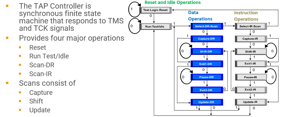
At the test-logic-reset controller state, the test logic is disabled to allow normal operation of the boundary scan device in its intended functional mode. The instruction register is initialized to contain the IDCODE instruction if the device contains the optional identification register or the BYPASS instruction. Regardless of the TAP controller state, it will enter test-logic-reset when test mode select (TMS) is held high for at least five rising edges of the test clock (TCK), or when the optional test reset pin (TRST) is asserted. The TAP controller remains in this state while TMS is high.
The run-test/idle state is a TAP controller state where once entered, the controller state will remain if the test mode state (TMS) is held low. In the run-test/idle state, only certain instructions are available. For example, the RUNBIST instruction causes a self-test of the boundary scan device system logic to execute. For instructions that do not cause functions to execute in the run-test/idle state, the test data registers selected by the current instructions will retain their previous state.
Each position in the Data Register and Instruction Register columns represents a state of the TAP Controller (the 16-state machine that controls each boundary-scan device). The states in the two columns vary only by the suffixes. These suffixes identify the column and the register operation that they affect.
Along the data flow lines connecting each tap state are numbers, a 0 or a 1. These numbers are the states of the TMS input signal required to move from one state to the next when TCK is sampled on its rising edge.
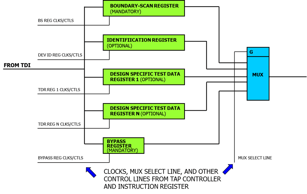
As observed in the TAP controller graphic, there are two types of registers present in boundary scan. The blue boxes represent the Data Register (DR), and the gray boxes represent the Instruction register. Each compliant boundary scan device has one Instruction register and two or more Data Registers. The primary data registers are the Boundary Scan Register (BSR) and the BYPASS register, which are both mandatory registers. Another possible data register is the IDCODE register which is optional. There may be other data registers, but they are not required by the boundary scan standard.
The three types of Data Registers are described below:
BSR – Primary testing data register. Transmits data to and receives data from the I/O pins of the device.
BYPASS – Single-bit register that passes information from TDI to TDO. This register shortens the path through the boundary scan device, allowing access to other devices in the scan chain to be tested.
IDCODE – Contains the identification code (ID code) for the device. The IDCODE is a 32-bit value which contains version, part number, and manufacturer information data for the device. The IDCODE is listed in the Boundary Scan Description Language (BSDL) file. This comparison of the IDCODE read from the device and what is listed in the BSDL file. This test is to ensure the proper device per the Bill of Materials (BOM) has been placed on the board.
The instruction register holds the current instruction the device will execute. When the instruction operation code (OPCODE) is shifted into the instruction register and decoded, the boundary scan device executes the instruction. Most often, the instruction executed determines which data register will be configured between the TDI and TDO pins. The output of each data register connects to an internal mux. When the instruction is executed, one of the data registers is configured between the TDI and TDO pins. The TDI-TDO path allows instruction data and serial data to enter the device and exit the device.
Each compliant boundary scan device can execute several mandatory instructions. There are also optional instructions the device manufacturer can choose to implement within the device.
Mandatory Instructions:
BYPASS – Places the single-bit data register to be connected between TDI and TDO. Serial data bypasses the Boundary Scan Register which shortens the path through the device.
EXTEST – Places the Boundary Scan Register to be connected between TDI and TDO. Test interconnects between boundary scan devices.
SAMPLE – Places the boundary scan register to be connected between TDI and TDO. Allows the device to remain in functional mode and samples device I/O signals.
PRELOAD – Places the boundary scan register to be connected between TDI and TDO. Allows the device to remain in functional mode. Shifts patterns to boundary scan devices while in functional mode.
Optional Instructions:
INTEST – Places the device in an internal boundary test mode and selects the boundary scan register to be connected between TDI and TDO.
RUNBIST – Places the device in self-test mode, enables a comprehensive self-test of its core logic and selects a user-specified data register to be connected between TDI and TDO.
CLAMP – Sets the outputs of the device to logic levels determined by the contents of the boundary scan register and selects the bypass register to be connected between TDI and TDO.
HIGHZ – Sets all the device outputs to a disabled (high-impedance) state and selects the bypass register to be connected between TDI and TDO.
IDCODE – Allows the device to remain in its functional mode and selects the optional device identification register to be connected between TDI and TDO.
USERCODE – Allows the device to remain in its functional mode and selects the optional device identification register to be connected between TDI and TDO. Captures user-defined information about the device.
Each instruction is defined by an OPCODE which is listed in the BSDL file. These OPCODES are shifted into the boundary scan device’s instruction register, decoded, then the decoded operation is executed.
During board layout, each boundary scan device is connected in what is commonly known as a board scan chain. An example of a printed circuit board scan chain is pictured below.
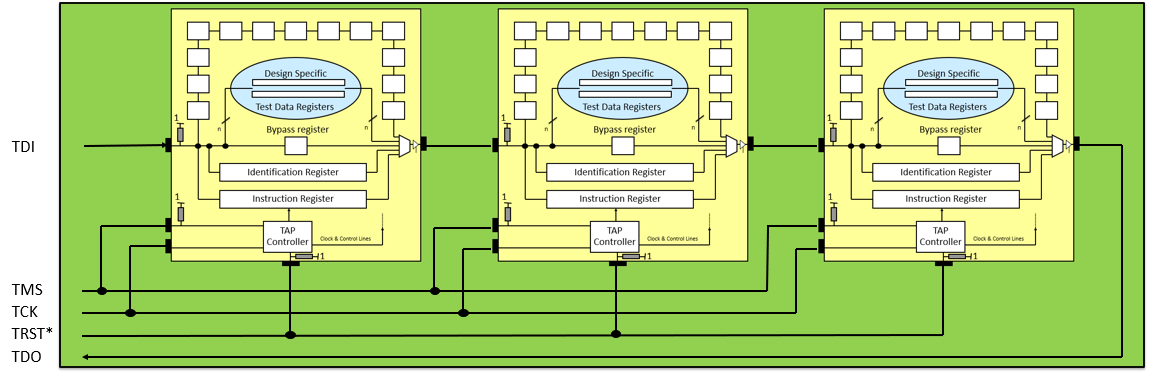
Through a printed circuit board edge connector, the TDI and TDO signals are connected in a serial fashion, boundary scan device to boundary scan device. The TMS and TCK signals are connected in a parallel fashion to each boundary scan device. The optional TRST signal is connected to each device if the pin is present. The TAP signals are applied to the printed circuit board via ScanWorks using an external pod.
Want to learn more about the basics of Interconnect and JTAG/Boundary Scan? Please read the first and second installment in this series; and for even more information, read our in-depth Boundary Scan Tutorial, Second Edition.
This is enough for now. In the next blog, we will continue our journey detailing everything you need to know about ScanWorks Interconnect.