
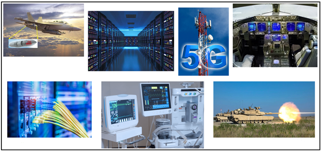
What is the meaning of the word “interconnect”? As the word is applied in the field of electronics, interconnect, as defined at Techopedia.com, defines the word as follows. “An interconnect (generally speaking) is a physical or logical connection between two electronic devices or networks.” Printed circuit boards (PCB) consisting of hundreds, sometimes, thousands, of interconnected integrated circuits (IC) and other active and passive devices are essential in today’s electronic world. Communication systems, defense, computers, medical devices, and aircraft, all rely on one or more PCBs that make their functionality possible.
As I stated in my previous blog, the complexity of PCBs has grown exponentially in the last 30+ years. This fact has presented unique challenges to the PCB test industry. However, no matter the complexity of the PCB, basic structural testing of the PCB must be implemented to ensure valid manufacturing processes and to determine if the PCB will function as designed.
The IEEE 1149.1 Standard for Test Access Port and Boundary Scan Architecture (also known as Boundary Scan or JTAG), introduced in 1990, presents a method of the testing complex PCBs while providing an opportunity for PCB designers and manufacturing engineers to increase PCB test coverage while reducing overall test cost. With Boundary Scan, PCB designers and manufacturing engineers can access embedded instrumentation within Boundary Scan ICs on PCBs through a 5-wire test bus. This test bus is known as the Boundary Scan IC’s TAP signals. The TAP signals are routed through the PCB, connecting the Boundary Scan ICs into a configuration called a Scan Chain.
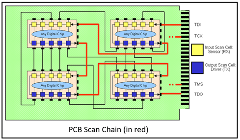
Boundary Scan provides a non-intrusive methodology of PCB testing. Utilizing the IEEE 1149.1 standard, ScanWorks facilitates structural testing of interconnects between ICs for open faults and short faults on PCBs.
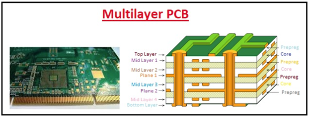
An open fault is simply a break in the electron conduction path. The open fault could be caused by an IC failure or a physical break in the conductor (also known as a trace or a net) during the PCB manufacturing process. Think of a trace or a net as wire connecting the ICs and other components (resistors, capacitors, switches, regulators, edge connectors, etc.) Some traces are visible because they are routed on the top and bottom layers of the PCB. However, a large majority of traces are not visible because they are routed on the multiple internal layers of the PCB. Although the overall thickness of PCBs is small (a few mm in overall thickness) there can be thousands of traces on the top, bottom, and internal layers of the PCB stack along with layers for PCB power and PCB ground planes.
Printed circuit boards (PCBs) are populated (or stuffed) quickly by pick-and-place machines which automate the placement of the components onto the PCB, while reflow ovens eliminate the need to solder each component connection separately. However, this high-speed manufacturing process is not immune to anomalies which is why a PCB testing strategy that can keep up with production is important. Slow testing can create a bottleneck in the manufacturing facility. No PCB testing could let defective products make it out of the facility and into the end-product.
As described earlier, an open fault is simply a break in the electron conduction path. The open fault could be caused by an IC failure or a physical break in the trace during the PCB manufacturing process. A short fault could be caused by an inadvertent splash of solder paste, erroneously connecting two pins together that are close to each other on an IC package or connecting across two or more nets during the manufacturing process. This is also known as a solder bridge.
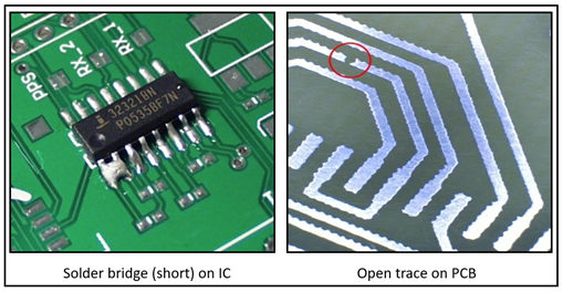
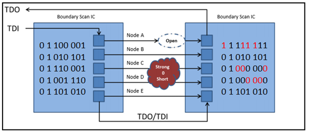
Short faults can also occur when solder touches a pin(s) and a voltage power rail or ground rail on the PCB. These faults could also be due to defects or anomalies during the manufacturing process.
Interconnect testing of PCBs is essential for a number or reasons. Without structural testing of PCBs, defects such as open faults or short faults could go undetected. If defective printed circuit boards are installed within their end-products, the product may not function properly (or not function at all) when used. Even if the product functions, with open for short defects present, its performance may begin to degrade over time to point where it becomes nonfunctional. Nonfunctioning products can lead to a high level of returns, which no company wants! Therefore, it makes sense to invest in proper testing of PCBs as a step in the manufacturing process instead of fielding a high level of returns on the backend.
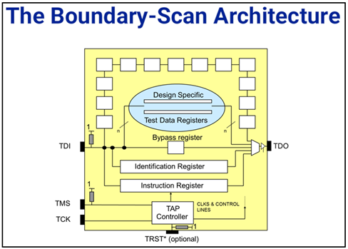
Before we create an Interconnect test action, we first create a baseline test to confirm our test infrastructure within each Boundary Scan IC is functioning properly. This test is called a Scan Path Verify action. Per the IEEE 1149.1 standard, Boundary Scan IC are designed with embedded registers. These registers perform specific Boundary Scan functions according to the 1149.1 standard as described:
- The Bypass Register is a one-bit value register that allows a shorter path through the IC
- The Instruction Register holds the instruction the boundary scan device will execute
- The Identification Register is a 32-bit register with encoded information specific to the device
- The Boundary Scan Register captures and/transmits test stimulus data
There can also be any number of design specific registers that permit advanced functions of the IC. These registers should be tested to ensure data can be properly captured from these registers, shifted into these registers, and that the registers update correctly. This process of Capture, Shift, and Update is governed by an embedded 16-state, state machine implemented into each Boundary Scan IC known as the Test Access Port (TAP). More to come on the TAP in the next blog. Boundary Scan devices, no matter the device manufacturer, have a similar internal architecture.
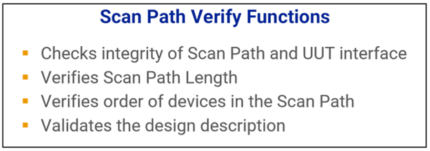
Once created, ASSET’s Scan Path Verify test action performs the following functions:
Well, I’ll wrap up this edition of the blog right here. In my next blog, we will explore the operation of the TAP controller, investigate the functionality of the various registers that comprise a Boundary Scan IC and describe how to create and apply the Scan Path Verify action to these registers.