
To tell the story of Interconnect, we must go back in time to the printed circuit board (PCB) test industry prior to the year 1990. At that time, electronics manufacturers relied upon a hands-on approach to test PCBs for structural integrity. Typical PCB test technologies of the time included the use of equipment such as in-circuit test (ICT), manufacturing defect analyzers (MDA), flying probe and X-ray machines.
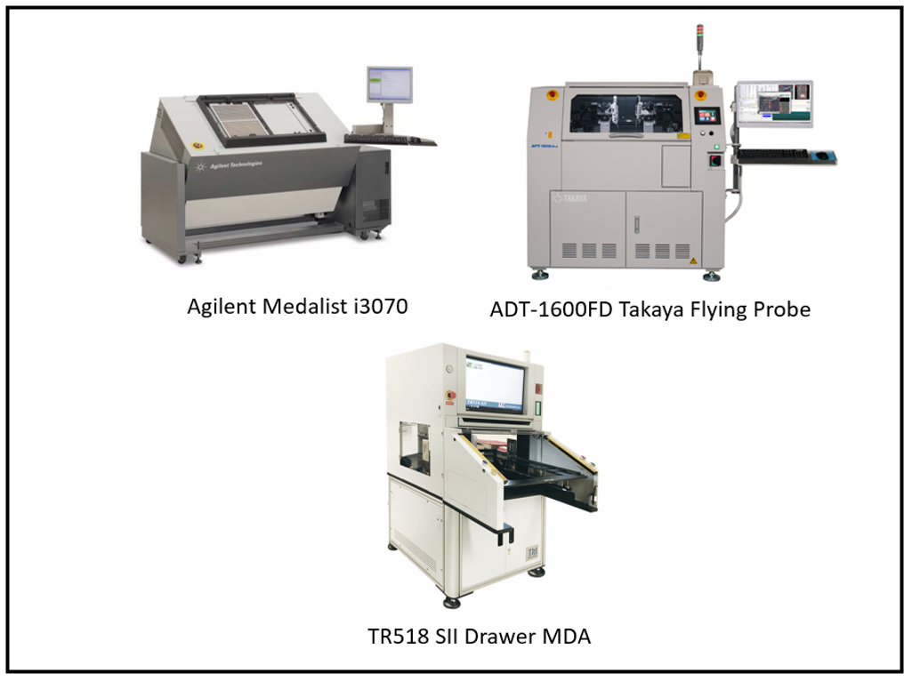
This equipment tended to be large, and if multiple testers were deployed, they would quickly begin to consume valuable space on the manufacturing floor. Also, these testers were expensive to purchase, and like any machine, required routine maintenance. Other external hardware used for PCB test were oscilloscopes and logic analyzers. While the PCB test methods and equipment/hardware required of this time were diverse, by nature, the implementation of each was dependent on actual physical contact with the PCB. This contact was primarily through the use of probes to test the PCB. Since all the methods required some degree physical contact to the test PCB, they were all classified into a category which became known as intrusive board test (IBT).
As stated, by their nature, IBT technologies such as ICT, MDA, flying probe, and others are hardware intense. These test methodologies rely on physical contact with the PCB. This is accomplished through the use of probes, sometimes referred to as nails. Expensive “bed-of-nail” fixtures and other hardware features were required for PCB test, along with and the necessary points of physical contact (test points) on the PCB itself. On some PCB designs of this time, a large amount of these test points were not related to the product mission or used in testing or commissioning. In summary, these test points were intrusive, and in many cases, pervasive.
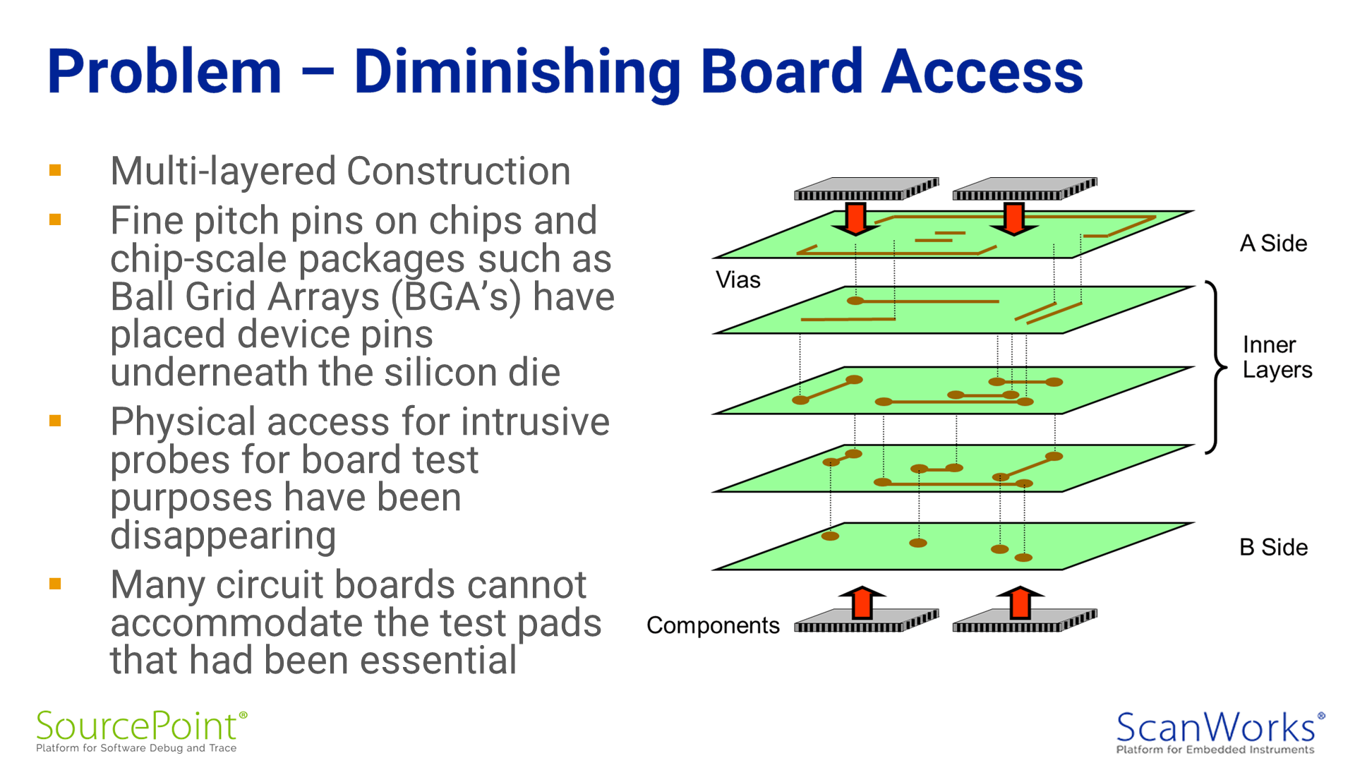
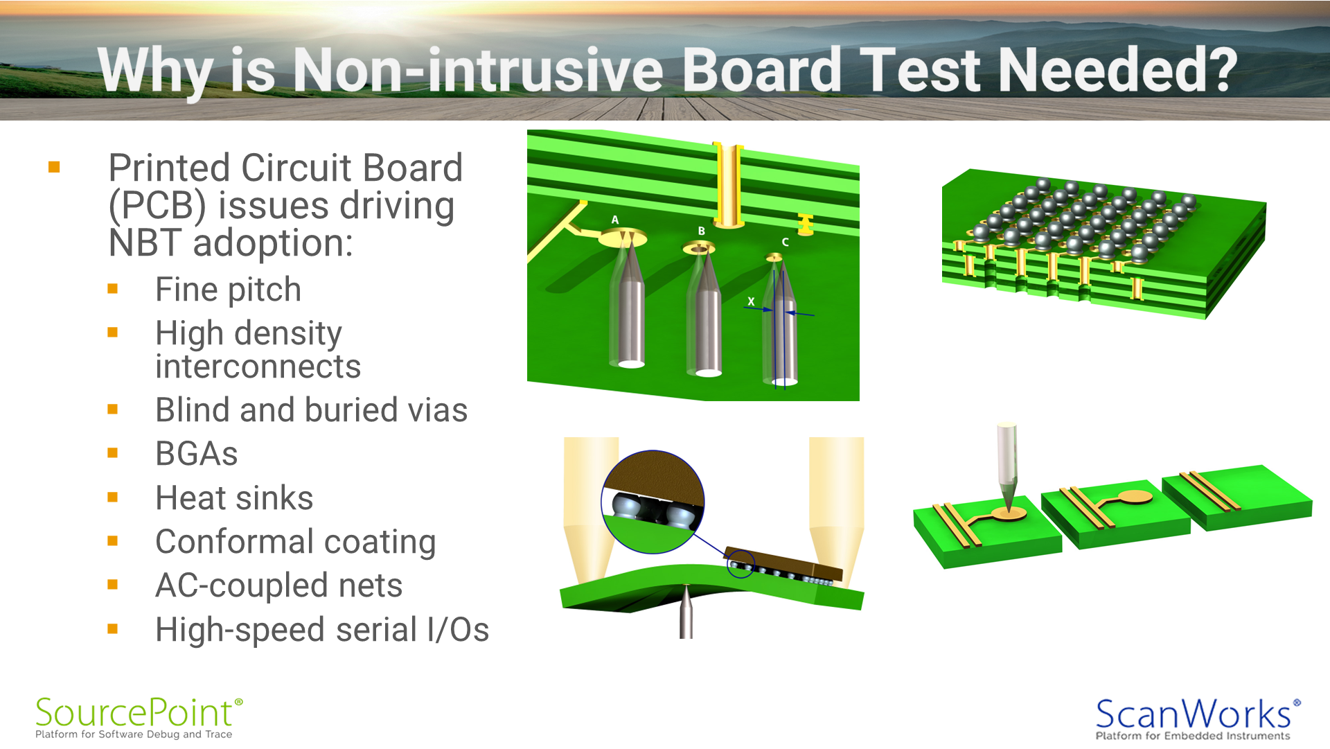
After 1990, significant changes in the PCB test industry began to take place. Electronic device packaging started becoming smaller and the use of Ball Grid Array (BGA) packaging began to increase. PCBs in turn, became smaller and were designed to support more devices. The speed of the devices on the PCB increased, and PCBs began to support more layers. The access needed by external instrumentation to physically probe PCBs has been diminishing significantly for quite some time now; faster and more complex chips with high-speed serial interconnects on dense boards with blind and buried via combine to make probing difficult, costly, and even prohibitive. Although these changes have advanced device technology and PCB design methods, these advances have decreased the access needed for PCB testing.
With all the aforementioned changes, a greater importance on a hands-off approach to test PCBs began to emerge. These test methods were classified as non-intrusive board test (NBT). NBT has become an increasingly essential facet of contemporary PCB test strategies. NBT requires less physical access to the PCB for testing. Recent developments in basic electronic technology, such as the disappearance of on-board test facilities and test points along with increasing IBT cost have combined to make NBT and the embedded instrumentation test technologies that comprise it a significant technology in the electronics manufacturing industry today.
As PCBs began to shrink in size, real estate on the PCB for test points begin to disappear. With this, capability for testing PCBs via intrusive methods began to decline. To maintain an adequate levels of test coverage in under these new conditions, a new method of testing was necessary.
A test method of structural testing was needed that was not reliant on test probes. A group of engineers known as the Joint Test Action Group (JTAG) began to address this problem.
From their subsequent meetings, they devised a test methodology that required little physical access to the PCB. This method depended on a 5-wire test bus running through the PCB that would allow access to the I/O need for testing without the need for test points. Later, this methodology was ratified as a standard by The Institute of Electrical and Electronics Engineers (IEEE) as what we know today as the 1149.1 Test Access Port and Boundary-Scan Architecture Standard.
NBT technologies such as Boundary Scan Test (BST) has become a necessity for proper PCB testing in large scale manufacturing facilities. NBT testing can be deployed without substantial increases to a corporation’s PCB test budget, as compared to IBT solutions.
In my next blog post, we will delve into the description of interconnect and the preceding steps and test actions required before creating an Interconnect action, specifically, what we call our ScanWorks Scan Path Verify (SPV) test. SPV test the Test Access Port (TAP) structural interconnects between the Boundary Scan devices on the PCB along with various registers associated with each Boundary Scan device. This test can uncover structural defects associated with the TAP signals and anomalies associated with the Boundary Scan registers. More to come on this so stay tuned for my next blog.