
I’ve had the opportunity to spend some time reviewing the 2013 Revision of the classic IEEE 1149.1 Standard. And, the technology introduced by this Standard is starting to make its way into the market. What is this technology, and why has it taken so long to gain adoption?
Those who might follow me via our blog site, or on social media, know that I’ve written on numerous technical topics over the years, ranging from silicon aging to signal integrity to firmware debug. All of these blogs originate from my experience with JTAG, the underlying technology behind low-level test, chip and printed circuit board design validation, and debug applications. JTAG originated on February 15th, 1990, when the IEEE Standard Board ratified the 1149.1-1990 – IEEE Standard Test Access Port and Boundary-Scan Architecture. IEEE 1149.1, also known as “JTAG” for the Joint Test Action Group that created it, is the specification that became the foundation of many other in-chip related technologies, such as:
1149.6 – IEEE Standard for Boundary-Scan Testing of Advanced Digital Networks
1532 – IEEE Standard for In-System Configuration of Programmable Devices
1149.7 – IEEE Standard for Reduced-Pin and Enhanced-Functionality Test Access Port and Boundary-Scan Architecture
1687 – IEEE Standard for Access and Control of Instrumentation Embedded within a Semiconductor Device
1838 – IEEE Standard for Test Access Architecture for Three-Dimensional Stacked Integrated Circuits
1149.10 – IEEE Standard for High-Speed Test Access Port and On-Chip Distribution Architecture
IEEE P2929 – Standard for System-level State Extraction for Functional Validation and Debug (C/TT/Scan and Array Debug)
and many more.
JTAG is ubiquitous; it is present in most devices of any level of complexity, as it is the foundation of low-level access and control of ICs.
One challenge for someone new to JTAG is obtaining the documentation at reasonable cost. The Standards are openly available, but at a cost. For example, the IEEE 1149.1-2013 standard can be obtained from www.techstreet.com at $301 for the PDF, and $361 for the printed edition. Even the original IEEE 1149.1-2001 is priced at $153 for the download. Discounts are available for paid IEEE members, and I’m all for supporting the IEEE, which does fantastic work for the industry. But, the pricing of the documentation is certainly better-suited to enterprises than to individual researchers or hobbyists on a budget. And not having the documentation “open source”, so to speak, does restrict its distribution.
So, in the interest of sharing what I’ve learned and making at least a general understanding of the technology more widely available, I’m going to outline basic JTAG (IEEE 1149.1-2001) first, then go over the innovations introduced by IEEE 1149.1-2013 from benefits and technology perspectives.
A stylized diagram of a chip with JTAG in it is below:
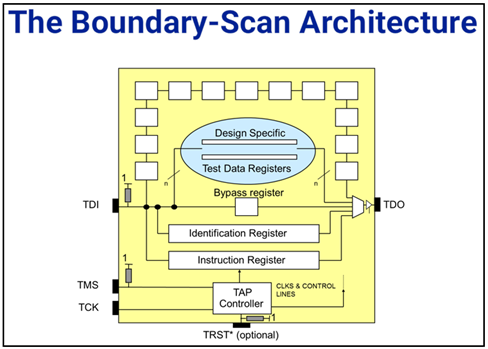
The architecture has the following main components:
A set of four dedicated test pins — Test Data In (TDI), Test Mode Select (TMS), Test Clock (TCK), Test Data Out (TDO) — and one optional test pin Test Reset (TRST*). These pins are collectively referred to as the Test Access Port (TAP).
A boundary-scan cell on each pin, connected internally to form a serial boundary-scan register.
A finite-state machine TAP controller with inputs TCK, TMS, and TRST*.
An n-bit (n >= 2) Instruction register, holding the current instruction.
A 1-bit Bypass register.
An optional 32-bit Identification register capable of being loaded with a permanent device identification code.
And a closer look at one of the boundary-scan cells, that make up the boundary register, is below:
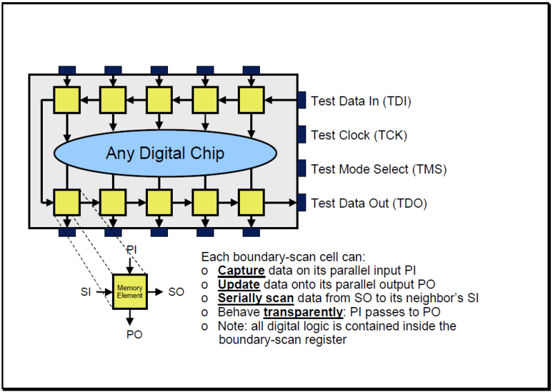
Note that there is some JTAG logic behind each pin, a boundary scan cell, that can not only shift data serially around the perimeter of the device, but also shift data between the pins interfacing to the outside world and the internal system logic. And, as an example of a boundary scan cell, consider the following:
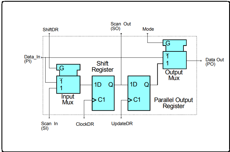
This example boundary scan cell has four modes of operation: Normal, Update, Capture, and Serial Shift. The memory element is a simple D-type flip-flop with front-end and back-end multiplexing of data.
During Normal mode, PI is passed transparently straight through to PO. In other words, JTAG sits in the background and does essentially nothing.
During Update mode, the content of the output register is passed through to PO. Data is sent to the outside world.
During Capture mode, the PI signal is routed to the shift register and the value is captured on the next ClockDR.
During Serial Shift mode, the SO of one register flip-flop is passed to the SI of the next via a hard-wired path.
Note that both Capture and Serial Shift operations do not interfere with the normal passing of data from the parallel-in (PI) terminal to the parallel-out (PO) terminal. This allows, at least in theory, the capture of operational values “on the fly” and the movement of these values for inspection without interference with functional modes of operation.
Capturing system logic data, transparently shifting data along the periphery of the device, sending traffic out of the device in a bare metal, out-of-band way….powerful, huh? This turns out to be very valuable for everything from printed circuit board manufacturing test to silicon performance validation.
I could write on this topic for ages, but for now I’ll just refer readers to more in-depth material. The next level of detail is best read in our eBook, JTAG and Boundary Scan Tutorial, Second Edition. For more detail beyond this, I can recommend Ken Parker’s The Boundary Scan Handbook, Fourth Edition (available on Amazon and other sellers); and then ultimately the IEEE specification itself.
After going through some iterations, the industry settled on the currently most widely deployed implementations of the IEEE 1149.1-2001 specification. When I started working for ASSET, there were often many challenges associated with silicon non-compliance to the Standard: quite frequently, the Boundary Scan Description Language (BSDL) files that described the boundary scan implementation within the chip were incorrect, or there were flaws in the chip designs that caused them to deviate from the standard. Semiconductor companies often (but not exclusively) relied on their EDA software vendors to insert and verify the JTAG logic within their devices, and these implementations were sometimes flawed. But, these deviations from IEEE 1149.1-2001 are very much a thing from the past.
Of course, no technology completely stands still. 1149.1 underwent a significant revision within the IEEE in 2013, to accommodate changes driven by increasing circuit density, heterogeneous integration, lower voltages, faster I/O, and demands for lower power consumption. Without some changes, IEEE 1149.1 was at risk of becoming obsolete.
The new specification is about twice the size, pages-wise, than the 2001 version. Of all the industry drivers that prompted the revision, power consumption was a key one. Lowering power usage is an important factor for many ICs, whether it relates to battery life on a cell phone, or being able to idle I/O pins with boundary scan cells on a large server SoC. In devices that have power domains capable of being powered down, it is important not to break the JTAG chain, as it may be in use. Thus, the concept arose of breaking the chain into segments, such that the boundary register could have different configurations at different times; and control of these excludable and selectable segments had to be provisioned for.
To accommodate the foreseen above requirements, new operational modes, register designs, instructions, and data registers were introduced. Specifically, the following additions to the 1149.1-2001 Standard were made:
- A test mode persistence controller that can keep the test mode active even if the active instruction does not force test mode. Three new instructions (CLAMP_HOLD, TMP_STATUS, AND CLAMP_RELEASE) support this controller.
- A new, optional instruction (ECIDCODE). This instruction supplements IDCODE and USERCODE and queries the Electronic Chip Identification value used to identify individual integrated circuits.
- A component initialization mechanism that allows more options in initializing components for test. Three new instructions (INIT_SETUP, INIT_SETUP_CLAMP, and INIT_RUN) support this mechanism.
- A new test data register (reset_select) that allows TAP-controlled reset functions for components. A new instruction (IC_RESET) supports this register.
- A recommended, but optional, TAP to test data register interface.
- Rules to support observe-only boundary-scan register cells. These can capture signal values fault conditions on target pins.
- Rules to support excludable boundary-scan register segments.
- Updates to the Boundary Scan Description Language definitions.
- Codification of Procedural Description Language (PDL). PDL is used to document the procedural and data requirements for some of the new instructions.
Rather than delving into the details of each of the above, I’ll conclude by detailing the changes to the boundary scan description language (BSDL) necessitated by the new features. The BSDL is the key linchpin between EDA insertion and verification tool suite, that creates the logic within the IC, and the test application like ScanWorks that parses the BSDL and implements the needed patterns correctly.
For IEEE 1149.1-2013, the requirement of BSDL being a “proper subset” of VHDL has been removed, and rather it is now specified as being based upon VHDL. And, the BSDL reserved words were increased by 66 additional entries, as below:
| Assembled_boundary_length |
| Boundary_segment |
| Broadcastfield |
| Broadcastvalues |
| Clamp_hold |
| Clamp_release |
| Default |
| DelayPO |
| Domain |
| Domain_external |
| Domctrl |
| Dompor |
| ECID |
| ECIDcode |
| Expect0 |
| Expect1 |
| Hierreset |
| IC_reset |
| Init_data |
| Init_run |
| Init_setup |
| Init_setup_clamp |
| Init_Status |
| Linkage_buffer |
| Linkage_in |
| Linkage_inout |
| Linkage_mechanical |
| Linkage_out |
| Mon |
| NoPI |
| NoPO |
| Noretain |
| NoUPD |
| One_hot |
| Open |
| Open0 |
| Open1 |
| OpenX |
| Power_0 |
| Power_pos |
| Power_neg |
| Power_port_association |
| Pulse0 |
| Pulse1 |
| Register_access |
| Register_assembly |
| Register_association |
| Register_constraints |
| Register_fields |
| Register_mnemonics |
| Reset_select |
| Resetval |
| Segment |
| Segmux |
| Segsel |
| Segstart |
| Selectfield |
| Selectmux |
| Selectvalues |
| Shared |
| Sysclock_requirements |
| TAPreset |
| Tie0 |
| Tie1 |
| TMP_Status |
| TRSTreset |
| User |
| Vref_in |
| Vref_out |
In a future blog, I’ll delve into some (but not all – that would make the article far too long!) of the above reserved keywords, and describe how they relate to some of the new key features provided by 1149.1-2013.