
A few weeks ago, I attended the International Test Conference (ITC) – the premiere annual event for semiconductor Design for Test (DFT). Like last year, the topic of Silent Data Corruption (SDC) was very hot; in short, SDC is a result of flaws within a semiconductor that causes invisible errors in the data that it processes. As one example of this, a CPU might erroneously calculate 1+1 and yield 3. I’ve been tracking this issue for several years, and here are my shared insights on the issue, our industry’s challenges, how we’re responding, and report from the conference.
SDC, sometimes referred to as Silent Data Error (SDE), has been recognized for decades, and is particularly onerous – the errors are “silent”, and are thus normally undetected. A single bit in a computation randomly flips. These sort of errors are of very low frequency, and are undetectable when they happen. One might ask, why is this an issue? Can’t unexpected bit flips be detected via checksums, such as the error correction code (ECC) mechanism in computer memory, or at the logic level via computational redundancy? That’s a good question. The short answer is that the errors occur at an extremely low level, in the silicon, in logic blocks for which there is no redundancy or checksums possible.
This technology issue also has huge business implications for the future of computing. It is recognized that SDC becomes more prevalent in large, complex silicon at advanced processing nodes. And the frequency of occurrence is higher in large datacenters – such as those within the cloud service providers. We have, over time, developed a high level of dependence and trust in computer calculations: we expect the balances in our bank accounts to be correct, for example, and not shifted left by a decimal place; and companies make billion-dollar decisions based upon computer-generated models. Trust in computing is based upon confidence in computational results. Break this, and we open up business disruptions, litigation, and other nasty side effects.
What is the frequency of these errors? Given that they are random and intermittent, a clear answer to this is not obvious. But, at ITC, it was anecdotally and generally recognized that “if you run a workload, like an AI Large Language Model with massively large data sets for a couple of months, you’re sure to see them.”
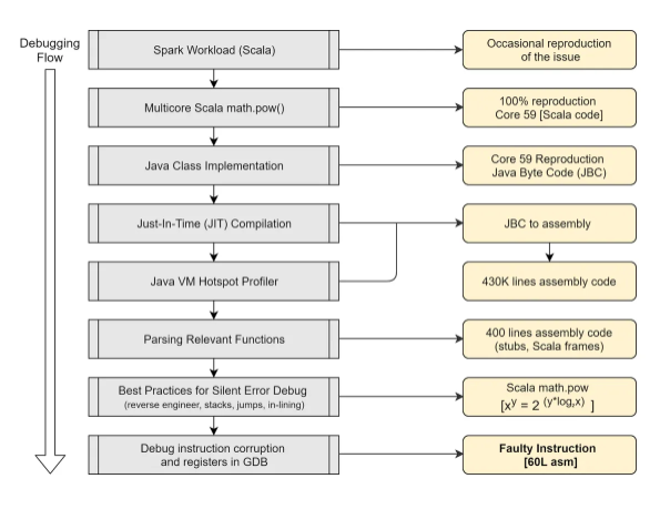
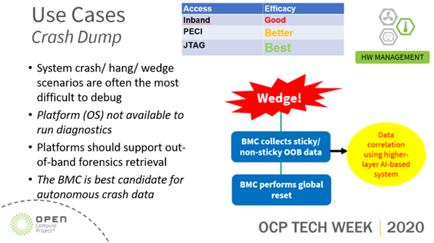
You might also ask, if these errors are silent, how do we even know they are happening? The fact is, we don’t, but we can run tests to induce them, and then sequester the devices that seem to exhibit them; as per the below diagram from Mitigating the effects of silent data corruption at scale, a calculation of INT(1.153) always yielded a result of 0 on Core 59 of a specific CPU. However, INT(1.152) would always result in the accurate value of 142 on this core. Note that as part of the debugging flow, it was determined that the problem could be induced by isolating down to 60 lines of assembly code:
What is the root cause of SDC? That’s not very clear at the moment. Intuitively, they can derive from two sources: transient faults, such as those induced by stray neutrons and other forms of radiation, and permanent faults, due to defects within ICs. The latter, or “time 0 defects”, present the biggest challenge, and will be the focus of the rest of this paper. It is generally understood that latent chip defects, such as resistive vias, combined with silicon aging, exacerbate the issue of SDC.
My interest in this topic dates back to 2012, when I wrote Margins (Eye Diagrams) follow the Silicon and Margins (Eye Diagrams) follow the Silicon – Part 2. Some images from these articles will capture the essence of the research we had done:
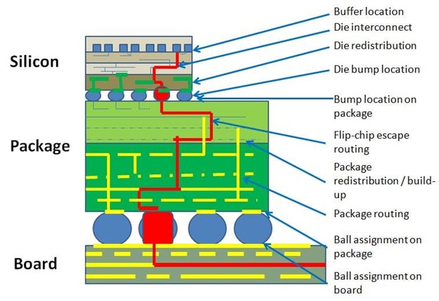
It’s clear from the above that small defects and marginalities at numerous points in a device could yield inconsistent results. We see the same effects at a printed circuit board level.
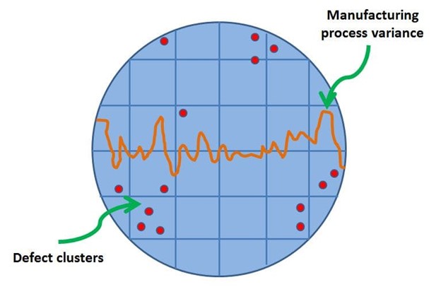
At a wafer level, defects tend to occur closer to the edge of the wafer due to manufacturing process variances there, and they tend to occur in clusters.
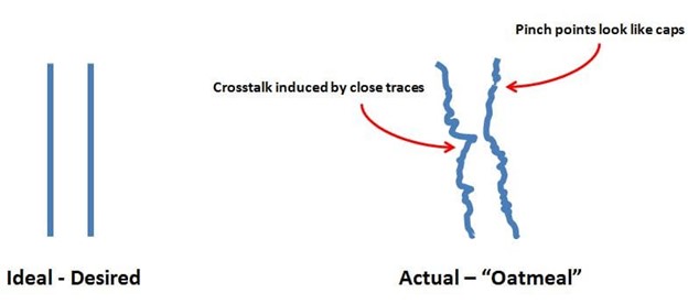
At a microscopic level, adjacent nets are not perfect, and exhibit irregularities in shape and size. This is the “oatmeal” effect:
I then followed up with Silicon Aging and Signal Integrity; the first sentence of which began as “Fruit rots. Tires wear out. And silicon ages, too.” The blog described reliability degradation due to the root causes of random telegraph noise (RTN), bias temperature instability (BTI) and hot carrier injection (HCI). Note that these were admittedly brief treatments of the topic – I have become more verbose in my writing as the years have gone by, as you can see. But the message is clear: there are marginalities everywhere within silicon, that become more apparent at smaller nodes; when operating conditions push the envelope in terms of process, voltage, temperature and frequency; and when silicon ages.
What is the industry doing about this? Up to now, to a great extent, most of the effort has gone into fleet-level functional testing to indict the chips that are more prone to generate SDC. Harish Dixit of Meta describes in his paper Detecting silent errors in the wild: Combining two novel approaches to quickly detect silent data corruptions at scale how they run a set of offline and online tests to catch the bit flips in action. Fleetscanner runs tests on any given server roughly every six months, when it is taken out of service for maintenance action, such as for firmware updates. But this is very slow: test time is in minutes, and so far they’ve consumed about four billion fleet-seconds doing this (this is time wasted when the server should be in service running workloads). And Ripple runs on production systems, stealing some cycles in the order of milliseconds, and the time to total fleet coverage is faster, about 15 days. But this test consumes about 100 million fleet seconds per month; again, time spent not generating revenue.
The semiconductor companies are starting to step up. Intel has led the charge with its DCDIAG functional test. As excerpted from the previous link, “Some people may ask why Intel is opening tools to find CPUs that wear out over time. We are confident in our CPU quality but understand that identifying CPUs that no longer function correctly is key to server fleet management.”. Impressive.
Additionally, as documented in Phoronix’s articles Intel “In-Field Scan” Coming With Sapphire Rapids As New Silicon Failure Testing Feature and Intel In-Field Scan Functionality Being Extended With Emerald Rapids. The Linux kernel update threads, as referred to in the prior two articles, are of particular interest. This solution encompasses both scan test and array test. But, as updates to the Linux kernel, they will presumably run under control of the operating system. This unfortunately retains the issue of stealing production workload cycles doing test. Not a good use of time and money. Clearly, two other approaches should be pursued: a design-oriented approach to eliminate the generation of SDC in the silicon, and also testing out-of-band without stealing production cycles.
I’ll write about the design-oriented approach later. For now, let’s consider running tests on in-system units independently and autonomously from the operating system, saving CPU cycles for real workloads.
I wrote about this topic initially as part of my participation with the Open Compute initiative. Back in 2017, Open Compute recognized the requirement for enhancing the debuggability of its whitebox servers by designing them with BMC connectivity to the selected CPU’s JTAG interface. The schematics for Project Olympus incorporating this capability were published then, and documented here: Microsoft Project Olympus Schematics and Embedded JTAG Run-Control. Some of the connectivity can be seen here:

Subsequently, there were a few different treatments of this topic. Sumeet Kochar of Lenovo (now with Oracle) did a 2019 OCP Summit presentation entitled Exploiting the true potential of At-Scale Debug which is viewable on YouTube: https://www.youtube.com/watch?v=XTxNLBf1MWk.
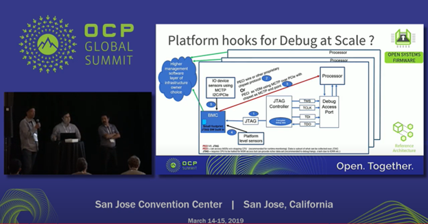
And during the pandemic in 2020, I presented Embedded JTAG debug of OCP Platforms at the OCP Tech Week, which is on YouTube here: https://www.youtube.com/watch?v=aXdBwCFUB_w: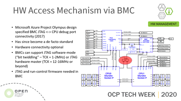
ASSET has productized the concept of using service processors, such as BMCs, to perform bare-metal, out-of-band debug and test on CPUs in the lab and in the field. There is a standard set of JTAG and run-control API provided by our ScanWorks Embedded Diagnostics (SED) offering that provides low-level access to functions such as scan test and array BIST, documented here: https://www.asset-intertech.com/products/scanworks/scanworks-embedded-diagnostics/.
Today’s BMCs, such as the ASPEED AST2600, are capable of up to 32MHz sustainable TCK via an on-chip JTAG HW Master function. More general information on this technology is available here: JTAG Hardware Master function for embedded test, debug, and device programming. Realistically, signal integrity limitations of the target hardware printed circuit board design’s debug interface limits these to about 20MHz. To deliver scan test, very large vectors (in the GB range) need to be delivered via a high-speed Test Access Port (HSTAP). For such higher speeds, BMCs typically have a x1 PCI Express Gen1 lane connected to a CPU, for management purposes. These could be repurposed to provide the gigabit speed HSTAP functionality required for true in-field, out-band scan test. Such solutions are being tested in the field now.
SDC is the big issue of our times. It’s going to take innovative, leapfrog initiatives in design and test to overcome it.