Fruit rots. Tires wear out. And silicon ages, too. Let’s look at the degradation process and its effects on chip signal integrity and performance.
As metal oxide semiconductor field effect transistors (MOSFETs) scale to ever-smaller geometries, speed and transistor density increase, while active power per transition decreases – all desirable in today’s world. But, the natural aging process becomes accelerated as this scaling continues. Let’s define aging in this context as being degradation in the signal integrity (SI) within a chip, which in turn leads to higher bit errors and reduced performance over time. Of course, aging will affect all attributes of a chip’s performance, but SI is of particular interest due to the significant impact to system overhead at higher levels of the stack when errors are introduced at the SerDes PHY layer.
A couple of sources of reliability degradation are:
- Charge trapping
- Electromigration
Some examples of charge trapping include RTN, BTI and HCI. An excellent article in EDN describes the effects of random telegraph noise (RTN) and bias temperature instability (BTI). RTN occurs when a hole or an electron is captured in an oxide trap and the captured charge is emitted from the trap. As this charge capture and charge emission continues, the
drain current (Id) fluctuates, which causes the threshold voltage (Vth) to shift. RTN gets worse with increasing temperature.
BTI is another example of charge-trapping which decreases Id and shifts Vth. BTI in particular has a permanent component, which almost never is recovered from.
Hot carrier injection (HCI) is a similar phenomenon where an electron or a “hole” gains sufficient kinetic energy to overcome a potential barrier necessary to break an interface state. This can result in damage to the encasing dielectric material if the hot carrier disrupts its atomic structure. The presence of such mobile carriers in the oxides triggers numerous physical damage processes that can drastically change the device characteristics over prolonged periods.
Charge trapping degrades the chip performance over time, until ultimately the thresholds collapse.
Another source of reliability issues within chip is electromigration within a chip’s interconnects. Electromigration is the transport of material caused by the gradual movement of the ions in a conductor due to the momentum transfer between conducting electrons and diffusing metal atoms. Although electromigration damage ultimately results in failure of the affected IC, the
first symptoms are intermittent glitches, which are almost impossible to diagnose. We have seen from previous blogs that differential pair used for I/O (within a chip and on a board) are in fact somewhat “self-healing”, in that open circuits may yet have sufficient coupling to allow successful data transmission – albeit at a higher error rate.
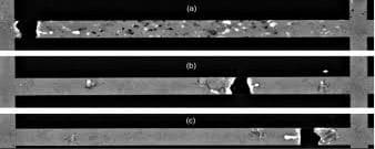
An electron microscope view of interconnect breakdown due to electromigration is below:
Certainly, the semiconductor industry intensively researches these reliability issues, and many mitigating technologies are in place to extend the life of ICs. As usual, it is a race between shrinking geometries, form factors and process nodes, offset by new technology innovation.
As would be expected, different ICs will have different levels of defects, variances and aging which affect the SI of any given design. In fact, ASSET conducted an empirical study of silicon variations in SI, and found that it follows the chips even more than it follows the circuit board. This study can be reviewed in the white paper, Margins (Eye Diagrams) Follow the Silicon.


