
ASSET licenses its JTAG (IEEE 1149.1) Hardware Master as Intellectual Property (IP) for ASIC designers to accelerate device performance for test, debug and device programming purposes. This blog describes the technical attributes and functionality of this IP.
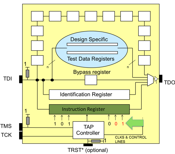
What is JTAG HW mastering? It’s a function within a chip that allows it to control and execute JTAG transactions on the scan chain attached to it. “Mastering” JTAG involves having the internal finite state machine (FSM) within a chip that supports operations such as state move, scan IR, scan DR, and others. The state machine looks like this:
Devices that support JTAG mastering may operate in either of two modes: what are commonly called software mode or hardware mode. Software mode basically consists of “bit-banging” or “pin-wiggling”, wherein the chip is made to cycle one TCK period while driving values on TDI and TMS, and returning the value of TDO. Chips without a dedicated JTAG hardware master burned into their silicon will use software mode, at the cost of poor performance (typically 1-2 MHz sustained TCK, which may be suitable for slower applications like test, but are unsuitable for debug forensics or device programming functions that retrieve a lot of data). JTAG hardware mode acts as an accelerated version of the software mode, by having the JTAG state machine functions in silicon logic, and batching up scans.
There are numerous chips out in the wild that have implemented software mode for JTAG mastering. Mostly, these have embedded SVF or STAPL players that are used, for example, to program subtending devices with small amounts of data.
There are also a small number of chips that implement hardware mode in the wild. The most notable is the ASPEED AST2600, that is fairly ubiquitously deployed as Baseboard Management Controllers (BMCs) on servers. On almost all servers deployed today, the AST2600 masters the CPU scan chain to perform at-scale debug functions. Examples of this use model are in the article Embedded API library for at-scale JTAG-based hardware-assisted debugging and the webinar recording At-Scale BMC-based debug of x86 servers.
With JTAG being as ubiquitous in chips of all shapes and sizes, and it being the gateway to all sorts of embedded instrumentation, having a JTAG master is table stakes for all sorts of applications. Among them are embedded test (see Embedded JTAG for boundary-scan test), embedded debug (see the links above), and in-system device configuration and programming. Applications for test and debug have been covered in many other articles (see above), so in this blog, I’ll focus on the device programming application. Having a higher-performance JTAG master for this is especially useful, given the large amounts of data used in configuring and programming today’s FPGAs and flash devices.
JTAG is the primary means of configuring FPGAs. A visual view of a typical topology is like this:
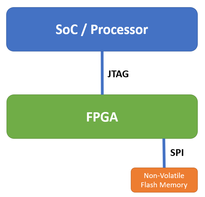
JTAG is the de facto standard access mechanism whereby FPGAs are configured. Of course, with FPGAs, the image programming is volatile and vanishes when power is removed. Often, the FPGA boot image is stored in a separate flash device and accessed with a Serial Peripheral Interface (SPI) bus or other. The JTAG interface may come into the FPGA board over a JTAG-to-USB converter, but it’s JTAG on both ends all the same. With FPGAs being ubiquitous in a huge number of industries, in anywhere from automotive to telecommunications, it’s important to have a fast, out-of-band mechanism to provide firmware updates, over-the-air (OTA) or otherwise. And with the increasing size of FPGA images (note that our RIC-1400 controller has an image of about 2MB; it is not unusual for larger FPGAs to have configuration data in the tens of megabytes) the need for speed is imperative.
The ASSET IP that implements the JTAG Hardware Master is a proven high-performance design that is utilized in all of ASSET’s off-the shelf-hardware offerings. The IP code is written in VHDL. It’s not unusual to have hardware mode operate 20X – 30X or more faster than software mode. A visual for a typical implementation topology is below:
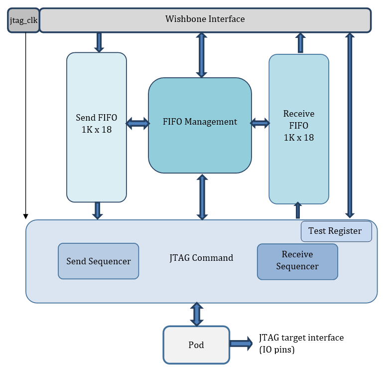
The module at the top presents a Wishbone slave to external modules (note that alternative ports, such as AHB-Lite, or such others with SRAM-like behavior, are also available). Commands and data issued to the module are directed to the Send FIFO. Data requested from the module is served by the Receive FIFO. Operations downstream of the FIFOs are synchronous to an applied jtag_clk that is distinct from the system clock that operates at the Wishbone interface (clk_i). Commands are processed in the JTAG Command module, which embraces the Send Sequencer for mastering the JTAG target interface and the Receive Sequencer for serving the return data. The Pod module mediates between these sequencers and the actual JTAG target interface (as presented at chip IO pins).
Wishbone Interface
This interface to higher level functions behaves like a standard Wishbone slave. The port comprises the following signals:
rst_i: Reset input
clk_i: Clock input (e.g. 100 MHz)
addr_i[9:0]: D-word (32-bit) aligned byte address
sel_i[3:0]: Select input array
cyc_i: Cycle input
stb_i: Strobe input
lock_i: Lock input
we_i: Write enable input
dat_i[31:0]: Data input array
err_o: Error output
ack_o: Acknowledge output
dat_o[31:0]: Data output array
One additional signal is required to originate from outside the module:
jtag_clk: JTAG source clock input
This is the direct source for the TCK output. As such, TCK frequency control, as may be required, is obtained by modifying the jtag_clk external to the module. ASSET can assist if highly flexible or granular TCK frequency control is required.
The JTAG Master IP is designed to operate with jtag_clk up to 50MHz and has no minimum frequency requirement, although a jtag_clk must be present for the JTAG Master IP to operate.
Provision of distinct jtag_clk allows reading and writing internal FIFOs and registers at much faster rates than the TCK is operating. This improves performance and frees the controlling processor to perform other tasks.
FIFO modules (send and receive)
Both FIFOs are organized with 1K depth by 18-bit width. Each FIFO location holds one 16-bit word of command or data with bit 16 as a flag indicating a command and bit 17 as a parity bit. Bit 16 in the receive FIFO will always be cleared since commands are only directed towards the JTAG controller. Each 32-bit read/write to the FIFO utilizes two 18-bit locations of FIFO. All associated registers are abstracted to the JTAG Command module.
FIFO management module
This module bridges the necessary FIFO controls and status to the Wishbone Interface and to the JTAG Command module. All associated registers are abstracted to the JTAG Command module.
JTAG Command module
The JTAG Command module is the heart of the JTAG Master IP, wherein all registers are abstracted and all commands are processed.
Pod module
The Pod module embraces the logic and signal conditioning necessary to mediate the JTAG target interface presented internally by the JTAG Command module with the JTAG target interface presented externally at the chip IO pins. The chip IO pins required are as follows:
TRST: Test Logic Reset output from JTAG Master
TCK: Test Clock output from JTAG Master
TMS: Test Mode Select output from JTAG Master
TDI: Test Data In (UUT referenced) output from JTAG Master
TDO: Test Data Out (UUT referenced) input to JTAG Master
The resources required by the JTAG Master IP are small when compared to today’s ASICs. The IP resides in fewer than 4,000 Lookup Tables (LUTs) (or equivalent) and require only 74k-bits of memory. These memory requirements are based on send and receive FIFOs sized at 2k by 18-bits. The following is a small excerpt from a place and route report of a similar implementation in a Xilinx Virtex-5 xc5vlx50t:
Number of Slice LUTS 3,682 out of 28,800 12%
Number of Slice LUT Flip-Flop pairs 5,177 out of 28,800 17%
The address space required by the JTAG Master IP is 256 32-bit locations of contiguous addresses within the ASIC.
Two global clock circuits will be required for routing the system and JTAG clock sources within the ASIC.
ASSET provides the source code, collateral and documentation associated with three main deliverables as part of these projects:
- JTAG Master RTL
- JTAG Master API
- JTAG Master exerciser/verifier
Let’s spend a minute highlighting the functions of the JTAG Master API. This is written in ‘C’, and the bus between the processor executing the API and the JTAG Master RTL can be any moderately high-speed parallel/serial bus with low latency. A table of the TAP controller features and function prototypes is as below:
| Feature | prototypes (e.g. from jtag_eie.h) |
| state move | int JTAG_EIE_API SetState(TAPSTATE endState); |
| state query | TAPSTATE JTAG_EIE_API GetState(void); |
| scan IR | int JTAG_EIE_API ScanIr(unsigned long count, unsigned long *tdi, unsigned long *tdo, TAPSTATE endState); |
| scan DR | int JTAG_EIE_API ScanDr(unsigned long count, unsigned long *tdi, unsigned long *tdo, TAPSTATE endState); |
| (max count) | “ |
| (null TDO) | “ |
| (no PAUSE) | “ |
| scan noRTI | int JTAG_EIE_API ScanDrNoRTI(unsigned long count, unsigned long *tdi, unsigned long *tdo, TAPSTATE endState); |
| scan noTMS | int JTAG_EIE_API Scan(unsigned long count, unsigned long *tdi, unsigned long *tdo); |
| enddr | endir | “ |
| (multipart scans) | “ |
| (hybrid tck) | “ |
| run tck | int JTAG_EIE_API RunTCK(unsigned long count, TAPSTATE endState); |
| run test | int JTAG_EIE_API RunTestTCK(unsigned long count, TAPSTATE endState); |
| trst onoff | int JTAG_EIE_API TrstOnOff(unsigned long mode); |
| TAP getset | unsigned long JTAG_EIE_API GetDISC_TAP_EN(void);
void JTAG_EIE_API SetDISC_TAP_EN(unsigned long enables); unsigned long JTAG_EIE_API ReadDISC_TAP_IN(void); unsigned long JTAG_EIE_API ReadDISC_TAP_OUT(void); void JTAG_EIE_API WriteDISC_TAP_OUT(unsigned long data); |
And finally, an excerpt from the jtag_eie header for a sample function like ScanDR, with comments, is:
int JTAG_EIE_API ScanDr(unsigned long count, unsigned long *tdi,unsigned long *tdo,TAPSTATE endState);

// Data scan function. This will move the state controller from its present location

// to SHIFT_DR and scan the desired number of bits, then move to requested endState.

// count = Total number of bits to be scanned

// tdi = Pointer to array containing the scan data to be output via JTAG.

// The first bit to be presented at TDI of the first device in the UUT

// scan chain should be the LSBit of tdi[0].

// tdo = Pointer to an array which will collect the scan data from TDO

// of the last device in the UUT scan chain.

// A NULL will be provided if no data is to be collected.

// The first bit collected will be stored at the LSBit of tdo[0]

// endState = State to navigate to once the shifting of data is complete.
And that’s it! Want to learn more? Drop me a note on LinkedIn or @AlanSguigna on Twitter.