
This blog post will take a deeper look at BSDL syntax and semantics errors and Scan Path Verify failures.
But before we dive in, if you missed part 7 of this series – where we covered the process of describing a Scan Path and creating a Scan Path Verify action in ScanWorks – here’s a quick recap:
- To begin, you must have the BSDL files for the Boundary Scan devices and you must know the proper order of the Scan Path on the board.
- The proper Scan Path order you’ll describe to ScanWorks begins with the Boundary Scan device closest to TDI and ends with the Boundary Scan device closest to TDO.
- Whether you have multiple Scan Paths with multiple TAPs on your board or have multiple Scan Paths using a Scan Path Linker device, with ScanWorks you can describe any configuration or number of Scan Path(s).
Once you import the BSDL files for your board, you’ll use the Build button to convert the BSDL files from their text format into a binary format for use by ScanWorks.
What if there is an error in the BSDL file(s)?
Fear not, ScanWorks has a built-in BSDL parser that examines the BSDL files for syntax and semantics errors during the build process. If an error is detected, a log is produced with the error description and the line number associated with the error. (An example of an error could be a missing semicolon (;) to end a line, or the wrong keyword used to describe a Boundary Scan cell type.)
Let’s look at a few logs so you’ll see how this works.
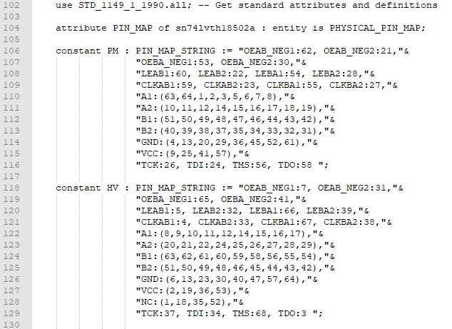
For this discussion, I’ve made an “edit” (inserted an error) to the PIN MAP section in the SN74LVTH18502A BSDL with a text editor.
Correct SN74LVTH18502A Pin Map
- Line 106: observe port OEAB_NEG1:62
- Line 119: observe port OEBA_NEG2:41 in the constant PM section
Incorrect SN74LVTH18502A Pin Map
- Line 106: observe that I changed port OEAB_NEG1:62 to OEAB_NEG:62
- Line 119: observe that I changed port OEBA_NEG2:41 to OEBA_NEG:41 in the constant PM section
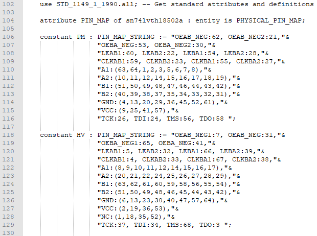
Now, you may think the edits I’ve made are trivial, however per the IEEE 1149.1 standard, names in the port section of the BSDL must match port names listed in the PIN MAP attribute section.
Nowadays, BSDLs are produced by Electronic Design Automation (EDA) tools, and errors like I have inserted, aren’t common. However, when BSDLs were created through manual processes (i.e., even by hand), BSDLs contained more errors in syntax and semantics. There were errors in cell descriptions, Boundary Scan Register sizes, instructions OPCODES, device package types, etc. Errors and inconsistencies exist in BSDLs so checking for correct syntax and semantics is important.
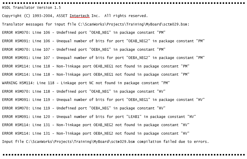
The next step is to Build the BSDL but, because of the edits, the BSDL for the SN74LVTH18502A will *not build* properly.
Error in SN74LVTH18502A BSDL
Let’s examine the log. For the time being, ignore anything that is marked by the word WARNING and only look for items preceded by the word ERROR.
BSDLs are provided by device vendors, and often may not be syntactically or semantically correct. Port names may be incorrect also. So, it is important to verify all BSDLs as correct.
The error messages tell us there is an undefined port on lines 106 and 119. You’ll see other errors because errors tend to cascade and cause other error messages. Working to eliminate the first error tends to elevate the following errors.
Fortunately, ScanWorks has a built-in editor that allows you to open the BSDL files that failed to build and make the necessary changes.
The remedy of course, in this situation, is to restore the numbers to the port names so they again match the port name listed in the port section of the BSDL.
If you encounter a BSDL that contains errors, you should inform the device manufacturer so they can correct it. Device manufacturers make their BSDLs available on their websites so they can be downloaded. This exposes an erroneous BSDL to many users so they should correct the BSDL quickly.
Before the manufacturer corrects the errors, the end user can make edits to the BSDL via the text editor to allow it to build so that project development can continue.
Connect a hardware pod
Once the BSDLs are built, and the ScanWorks Design Wizard has been used to arrange the Boundary Scan devices from TDI to TDO, it’s time to create and run the Scan Path Verify action.
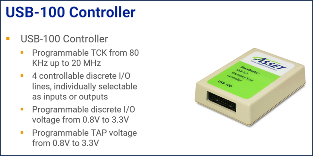
But before running the action, you’ll need an ASSET hardware pod. For example, ASSET’s most universal pod, the USB-100 controller.
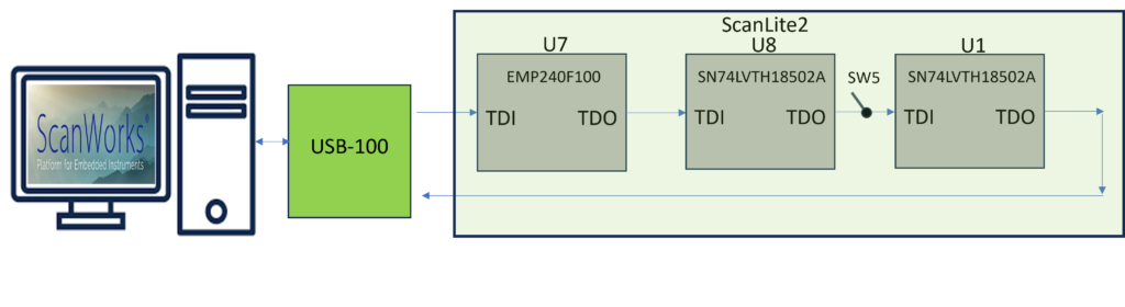
We’ll connect the USB-100 pod to the ScanLite2 board via a UUT test cable.
The Scan Path Verify action
The Scan Path Verify action runs each of these operations in the order listed on the Describe Scan Path UI.
Let’s look at the first 3 options:
- Device ID and Bypass DR Scan Only
- Instruction Capture
- BYPASS
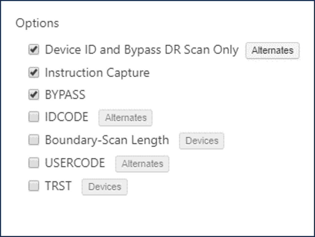
The options can be selected and run individually or all at once. Below is a description of the first three options.
| Option | Description |
| Device ID and Bypass ID | Device ID and Bypass DR Scan only test all components in the scan path. The initial action reset places the Device ID or Bypass register in the scan path for each device. A DR scan is done to check that the correct value from the ID code or Bypass register matches those defined in your BSDL description, in the order described in the scan path. The Alternates… button allows you to specify alternate ID codes that are valid for this design. |
| Instruction Capture | Instruction Capture checks the instruction register capture value for all components in the scan path using IR scans with the BYPASS instruction. This verifies that the instruction register for each device is functioning correctly. |
| BYPASS | BYPASS checks the TDI, TDO, TMS, and TCK signals in your scan path. An IR scan is done while devices are put into BYPASS during this test. A DR scan pattern containing zeros and ones is done. |
To demonstrate the error messages produced by ScanWorks, I’ll run each option and create a “break” in the Scan Path” by flipping switch 5 (SW5) on ScanLite2.
A break (open) in the Scan Path on the TDI to TDO path prevents data from being shifted through the Scan Path from the devices before it. Faults such as opens and/or shorts on the TAP nets can occur during the manufacturing process. With this “break”, we can anticipate that device U7 and U8 will fail most of the Scan Path Verify test. Opens and/or shorts can occur on other TAP signals as well. This is why the first Boundary Scan test that is created when using ScanWorks is the Scan Path Verify test. This test ensures that all the Boundary Scan devices are operating correctly.
Device ID and Bypass ID
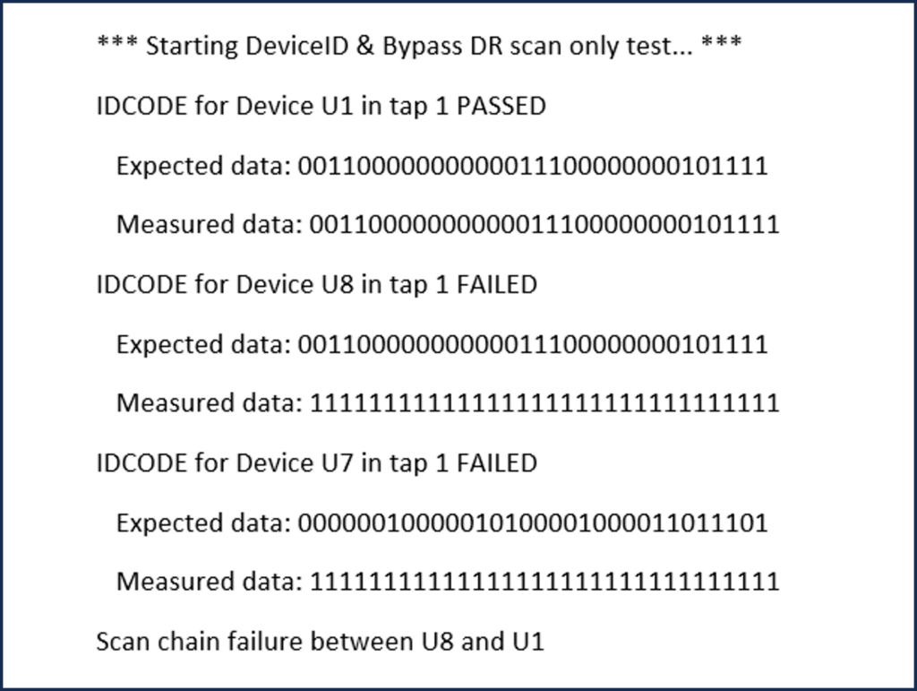
The first option we’ll run is DeviceID and DRscan only. Running the option with SW5 in the normal position creates the log below.
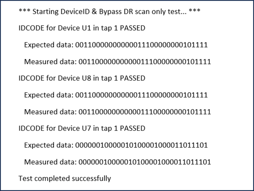
The IDCODES for the Boundary Scan devices match (Expected Data and Measured Data). Take note of the order the data is presented. U1 is presented first and U7 is presented last. Referring to the ScanLite2 diagram, you’ll observe that U1 is the device nearest TDO. As data is shifted out, the device nearest TDO data is received back at ScanWorks first. U7 is closest to TDI so its data comes out of TDO last.
Now we’ll open the switch then with it in position that creates an open.
When a Boundary Scan device powers up or is reset, either the IDCODE (optional register) or the BYPASS register (mandatory register) will be automatically configured between TDI and TDO internally. If the IDCODE register exists, it will be configured between TDI and TDO. The DeviceID and Bypass DR scan only option scans out the contents of the register configured between TDI and TDO. Again, this will be either the IDCODE register (32-bit register) or the BYPASS register (1-bit register). Scanning out this value exercises the Boundary Scan devices through the CAPTURE, SHIFT, and UPDATE states described in part 4 (Everything You Need to Know About ScanWorks Interconnect Part 4: The Test Access Port (TAP) State Machine). From the log file, it’s evident that each Boundary Scan device on the ScanLite2 has the optional IDCODE register.
We see that device U7 passed but U8 and U1 failed. Why? Well, this is due to the “break” open in the Scan Path caused by opening SW5. Another question, why are there 1s in the Measured row? Well, on the TDI input of every Boundary Scan device, there is an equivalent of a pull-up resistor internally. This means that when the TDI input is open or floating, a logic-1 is present. A logic-1 on the TDI keeps the device in a safe state. In this instance, logic-1 will be shifted through the Scan Path after the first 32 bits of device U1 are shifted. Since there are 3 Boundary Scan devices in the Scan Path of the ScanLite2, and each IDCODE register is 32-bit, the TCK will run for 96 clock cycles to shift out the IDCODE for the entire Scan Path.
Instruction Capture
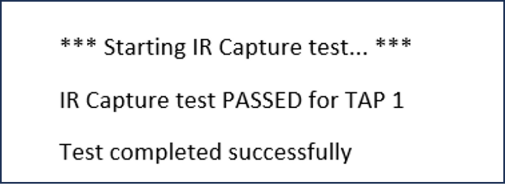
The next option is the Instruction Capture. With SW5 closed, the log below is produced. The Instruction Capture value is a hardwired value inside of the device. The log below indicates the Instruction Capture values for the devices have been captured, shifted back to ScanWorks, and compared to the Instruction Capture values in the BSDL without mis-compare.
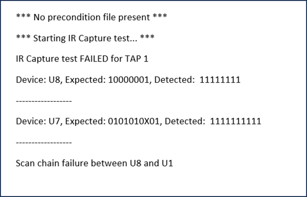
This log is with the SW5 open, and the Instruction capture option is run again. As expected, devices U7 and U8 fail because of the open switch. There is even a message stating that the failure is due to a failure between devices U8 and U1. The Expected and Detected data for U8 and U7 mis-compare. The Expected data never makes it back to ScanWorks.
BYPASS
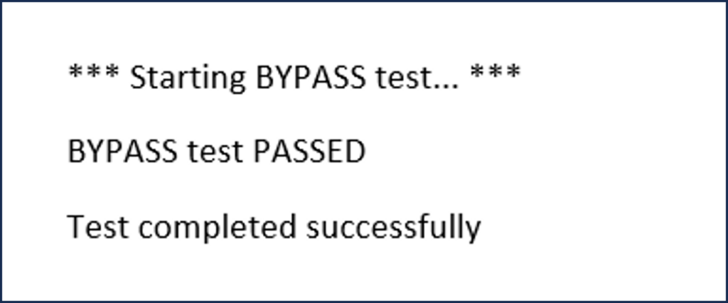
Lastly, we’ll run the BYPASS option. Again, with SW5 closed the log produced indicates all the BYPASS registers of each Boundary Scan device pass. The difference between this BYPASS option and the Bypass in the DeviceID and Bypass DRscan only is this option shifts in the BYPASS instruction into the Scan Path and places each device into the CAPTURE, SHIFT, and UPDATE states we discussed in previous blogs to configure the BYPASS register between TDI and TDO.
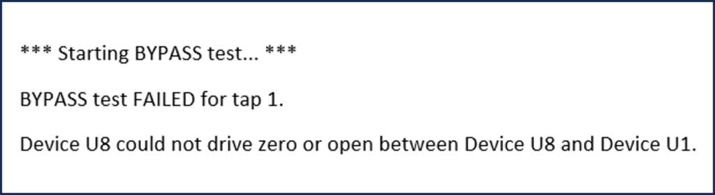
Now, with SW5 open, we get a message saying the BYPASS test failed. Running this option accurately identifies the open between U8 and U1 as well. The message states that ScanWorks could not drive a logic-0 or is open between Device U8 and U1. The BYPASS register has a hardwired logic-0 on its parallel input that it attempts to drive during the BYPASS test. This indicates that the logic-0 is not received at ScanWorks for U7 and U8.
The Scan Path Verify action and its options ensure the Boundary Scan devices on the board and their registers are operational.
ScanWorks does a great job of identifying problems with the Scan Path. The “break” in the Scan Path that I created is one of many problems that can occur with an onboard Scan Path.
There can be problems with any of the TAP signals or even the registers internal to the Boundary Scan devices themselves. No matter the problem, the ScanWorks Scan Path Verify action will find and identify the problem.
In the next blog, we’ll examine more Scan Path Verify options and output logs.