
In my previous blog. IEEE 1687 (IJTAG): ICL and PDL Explained, I provided a layman’s introduction to the Instrument Connectivity Language (ICL) and Procedural Description Language (PDL). As you may have gleaned from this article, ICL in particular is a complex language; its basic function is to describe the access network between embedded instruments and device interfaces. In this article, I’ll describe how an ICL network and instrumentation is created and inserted within a test FPGA, thereby giving more insight into the language’s constructs and the principles of IJTAG.
With our ScanWorks product, we demonstrate the use of IJTAG with a simple Project that we described in the previous article, using the Opal Kelly board. This ScanWorks Project stores (1) the board topology (that is, understands the layout of the Scan Path and the boundary scan attributes of the Xilinx Spartan-6 FPGA), (2) the SVF that programs and initializes the IJTAG network and the simple register/instrument that controls an LED, and (3) the ScanWorks Actions (vectors) used to run the PDL against the specific instrument.
The three ScanWorks Actions associated with our demonstration Project can be seen below:
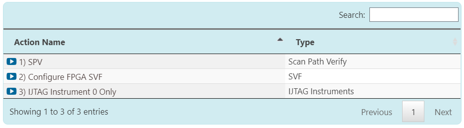
Action #1 above shows the Scan Path Verify (SPV). This Action is typically included in all Projects, as it’s the first action to run to verify scan chain integrity.
Action #2 above is used to insert the IJTAG network into the Spartan-6 FPGA.
And Action #3 above uses ICL and PDL to generate test actions using specific IJTAG iProcs against the instrument’s fully qualified network path. This is sometimes called retargeting, whereby a sequence of operations written in PDL are applied at the instrument boundary and mapped through the instrument access network to a higher level of hierarchy (and ultimately to the ports of the top-level module that connects to the Spartan-6’s pins).
What does the overall flow of creating these Actions and using them within ScanWorks look like? Here’s a visual of the flow, and I’ll describe the necessary steps:
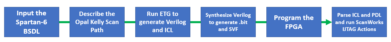
The first two steps, reading the Spartan-6 FPGA’s BSDL into ScanWorks and describing the board scan path, are standard steps that are done for all JTAG and boundary scan related projects.
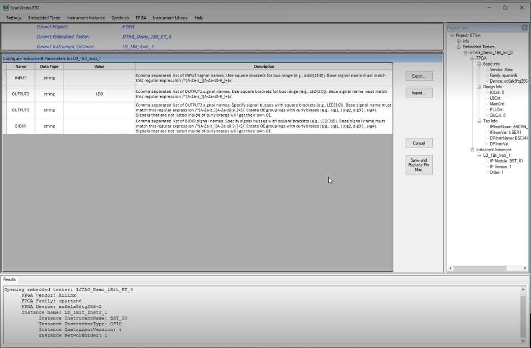
Note the third step, “Run ETG to generate Verilog and ICL”. ETG is short for Embedded Tester Generator, an application within ScanWorks that is used to create and install embedded instruments and provide access to them via an on-chip IJTAG network. For this example single-instrument Project, we are using a very simple instrument that is manifested by a single boundary scan cell. We need to do only two things: (1) configure the instrument based upon its defined attributes, and (2) associate the instrument with a pin map on the board. In terms of configuring the instrument, we are just defining an OUTPUT2 boundary scan cell – that is, the simplest 2-state output cell, since we will just be using it to turn the associated LED on and off:
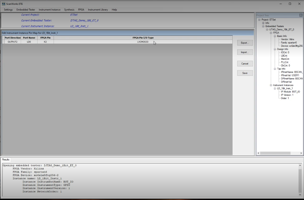
And regarding the pin, we know from the schematics of the Opal Kelly board that pin K2 is the one we’ll be using to light up its associated LED, so we set that up as well, calling its port LD0 (for later use in the ICL and PDL), and its I/O Type is known to be LVCMOS33:
Once this is done, we run ETG, that outputs the associated ICL and Verilog for the network and instrument. The Verilog RTL is below:
module LD_1Bit_Instr_1__Wrapper #(

  parameter            OUTPUT2 = 0

)(

  input  wire          ckDR,

  input  wire          ON,

  input  wire          shDR,

  input  wire          TCK,

  input  wire          TCK_B,

  input  wire          TDI,

  input  wire          TRST_B,

  input  wire          upDR,


  output wire          LD0,

  output wire          TDO

);


  // Wrap Input Wires

  wire                 xi_LD0;


  // Instrument Type Specific Wires

  wire                 TDO_ctrl;

  wire                 TDO_read;

  wire                 TDO_RW_mux;

  wire                 TDO_sib;

  wire                 TDO_write;

  wire                 WS_SEL;

  wire                 WS_SEL_ON;

  wire                 WSIo;


  my_and2 WS_SEL_enable ( .I0(ON), .I1(WS_SEL), .O(WS_SEL_ON) );


  sync_TypeSIB_1bit SIB

  (

    .ckDR(ckDR),

    .ON(ON),

    .shDR(shDR),

    .TCK(TCK),

    .TCK_B(TCK_B),

    .TDI(TDI),

    .TDO(TDO_sib),

    .TRST_B(TRST_B),

    .upDR(upDR),

    .WSIo(WSIo),

    .WSOi(TDO_write),

    .WS_SEL(WS_SEL)

  ); // SIB


  sync_TypeW_1bit Write_Data

  (

    .ckDR(ckDR),

    .NDO(xi_LD0),

    .ON(WS_SEL_ON),

    .shDR(shDR),

    .TCK(TCK),

    .TCK_B(TCK_B),

    .TDI(WSIo),

    .TDO(TDO_write),

    .TRST_B(TRST_B),

    .upDR(upDR)

  ); // Write_Data


  my_buf TDO_buf ( .I(TDO_sib), .O(TDO) );


  BST_IO_LD_1Bit_Instr_1

  #(

    .OUTPUT2(OUTPUT2)

  )

  LD_1Bit_Instr_1

  (

    .LD0(LD0),

    .xi_LD0(xi_LD0)

  ); // LD_1Bit_Instr_1


endmodule // LD_1Bit_Instr_1__Wrapper


module sync_TypeSIB_1bit

(

  // An IJTAG Segment Insertion Bit test data register that responds to the Synchronous JTAG signals


  input  wire         ON,

  input  wire         TDI,

  input  wire         WSOi,

  input  wire         TCK,

  input  wire         TCK_B,

  input  wire         TRST_B,

  input  wire         shDR,

  input  wire         ckDR,

  input  wire         upDR,


  output wire         TDO,

  output wire         WS_SEL,

  output wire         WSIo

);


  wire                i_shDR;

  wire                i_ckDR;

  wire                i_upDR;


  my_and2 shDR_enable ( .I0(ON), .I1(shDR), .O(i_shDR) );

  my_and2 ckDR_enable ( .I0(ON), .I1(ckDR), .O(i_ckDR) );

  my_and2 upDR_enable ( .I0(ON), .I1(upDR), .O(i_upDR) );


  sib_cell bit_0 ( .WS_SEL(WS_SEL), .WSIo(WSIo), .WSOi(WSOi), .TDO(TDO), .TDI(TDI), .TCK(TCK), .TCK_B(TCK_B), .TRST_B(TRST_B), .shDR(i_shDR), .ckDR(i_ckDR), .upDR(i_upDR) );


endmodule // sync_TypeSIB_1bit


module sync_TypeW_1bit

(

  // An IJTAG Shift-Update test data register that responds to the Synchronous JTAG signals


  input  wire         ON,

  input  wire         TDI,

  input  wire         TCK,

  input  wire         TCK_B,

  input  wire         TRST_B,

  input  wire         shDR,

  input  wire         ckDR,

  input  wire         upDR,


  output wire         TDO,

  output wire         NDO

);


  wire                i_shDR;

  wire                i_ckDR;

  wire                i_upDR;


  my_and2 shDR_enable ( .I0(ON), .I1(shDR), .O(i_shDR) );

  my_and2 ckDR_enable ( .I0(ON), .I1(ckDR), .O(i_ckDR) );

  my_and2 upDR_enable ( .I0(ON), .I1(upDR), .O(i_upDR) );


  sub_cell bit_0 (.TCK(TCK), .TCK_B(TCK_B), .TRST_B(TRST_B), .shDR(i_shDR), .ckDR(i_ckDR), .upDR(i_upDR), .NDO(NDO), .TDI(TDI), .TDO(TDO) );


endmodule // sync_TypeW_1bit


module IJTAG_Network

(


  input  wire          ckDR,

  input  wire          ON,

  input  wire          shDR,

  input  wire          TCK,

  input  wire          TCK_B,

  input  wire          TDI,

  input  wire          TRST_B,

  input  wire          upDR,


  output wire          LD_1Bit_Instr_1___LD0,

  output wire          TDO

);


  wire                 WSIo;

  wire                 WSOi;

  wire                 WS_SEL;


  LD_1Bit_Instr_1__Wrapper

  #(

    .OUTPUT2("LD0")

  )

  LD_1Bit_Instr_1__W1

  (

    .LD0(LD_1Bit_Instr_1___LD0),

    .ON(WS_SEL),

    .ckDR(ckDR),

    .shDR(shDR),

    .TCK(TCK),

    .TCK_B(TCK_B),

    .TDI(WSIo),

    .TDO(WSOi),

    .TRST_B(TRST_B),

    .upDR(upDR)

  ); // LD_1Bit_Instr_1__W1


  sync_TypeSIB_1bit SIB

  (

    .ckDR(ckDR),

    .ON(ON),

    .shDR(shDR),

    .TCK(TCK),

    .TCK_B(TCK_B),

    .TDI(TDI),

    .TDO(TDO),

    .TRST_B(TRST_B),

    .upDR(upDR),

    .WSIo(WSIo),

    .WSOi(WSOi),

    .WS_SEL(WS_SEL)

  ); // SIB


endmodule // IJTAG_Network


module ET_IJTAG_Demo_1Bit_ET_0

(

  output wire          LD_1Bit_Instr_1___LD0

);


  wire         tdi;

  wire         tdo;

  wire         cdr;

  wire         sdr;

  wire         udr;

  wire         tlr;

  wire         ckDR = (cdr || sdr);

  wire         shDR = sdr;

  wire         upDR = udr;


  // Xilinx BSCAN Interface specific wire declarations and signal assignments.

  wire         tck;

  wire         tck_b;

  wire         tms;

  wire         rti;


  wire         user_1_sel;

  wire         BSCAN_tck;


  BUFG BUFG_tck   (.O(tck),   .I(BSCAN_tck));

  BUFG BUFG_tck_b (.O(tck_b), .I(~BSCAN_tck));


  // Xilinx BSCAN Interface instance.

  //   Instantiate a "BSCAN_SPARTAN6" type JTAG interface

  BSCAN_SPARTAN6 #(.JTAG_CHAIN(1)) BSCAN_SPARTAN6_i (

      .CAPTURE(cdr),

      .RESET(tlr),

      .RUNTEST(rti),

      .SEL(user_1_sel),

      .SHIFT(sdr),

      .TCK(BSCAN_tck),

      .TDI(tdi),

      .TMS(tms),

      .UPDATE(udr),

      .TDO(tdo)

  ); // BSCAN_SPARTAN6_i


  IJTAG_Network IJTAG_Network_1

  (

    .ckDR(ckDR),

    .ON(user_1_sel),

    .shDR(shDR),

    .TCK(tck),

    .TCK_B(tck_b),

    .TDI(tdi),

    .TRST_B(tlr),

    .upDR(upDR),

    .LD_1Bit_Instr_1___LD0(LD_1Bit_Instr_1___LD0),

    .TDO(tdo)

  ); // IJTAG_Network_1


endmodule // ET_IJTAG_Demo_1Bit_ET_0


module IJTAG_Demo_1Bit_ET_0

(

  output wire           K2

);


  wire         LD_1Bit_Instr_1___LD0;


  assign K2       = ~LD_1Bit_Instr_1___LD0;


  ET_IJTAG_Demo_1Bit_ET_0 ET_IJTAG_Demo_1Bit_ET_0_i

  (

    .LD_1Bit_Instr_1___LD0(LD_1Bit_Instr_1___LD0)

  ); // ET_IJTAG_Demo_1Bit_ET_0_i


endmodule // IJTAG_Demo_1Bit_ET_0
It’s an exercise for the student to read this Verilog and piece it together. Have fun!
The ICL is also output by ETG. The contents are displayed in the previous article as well, but I’ll list it here for completeness. Here it is:
// The Instrument to be Tested

Module BST_IO_LD_1Bit_Instr_1__LD_1Bit_Instr_1

{

    DataInPort xi_LD0;

    DataOutPort LD0;

}


// SIB/TDR Unit: Contains an instance of the Instrument to be Tested,

//   the Test Data Register (TDR) associated with the Instrument, and

//   the SIB used to insert the TDR data into the Scan Chain.

Module LD_1Bit_Instr_1__Wrapper

{

    // Scan Chain associated ports

    ScanInPort TDI;

    ScanOutPort TDO { Source SIB_mux; }


    // Instrument associated port

    DataOutPort LD0 { Source LD_1Bit_Instr_1.LD0; }


    // Instance of the Instrument to be Tested

    Instance LD_1Bit_Instr_1 Of BST_IO_LD_1Bit_Instr_1__LD_1Bit_Instr_1 {

        InputPort xi_LD0 = Write_TDR[0];

    }


    // The Test Data Register (TDR) associated with the Instrument

    ScanRegister Write_TDR[0] {

        ResetValue 1'b0;

        ScanInSource SIB;

        CaptureSource LD_1Bit_Instr_1.LD0[0];

    }


    // The ScanRegister and ScanMux, collectively, comprise the SIB

       // (Segment Insertion Bit).  When the value of SIB is '0', the

       // SIB is considered "closed" and the TDR data cannot be accessed.

       // When the SIB is '1', the SIB is considered "open" and the TDR

       // data is inserted into the Scan Chain.


       // -- The SIB bit

    ScanRegister SIB {

        ResetValue 1'b0;

        ScanInSource TDI;

        CaptureSource SIB;

    }


    // -- The SIB MUX

    ScanMux SIB_Mux SelectedBy SIB {

        1'b0 : SIB;

        1'b1 : Write_TDR;

    }

}


// This Module defines the Scan Chain which includes any module

// instances that consist of Instrument TDRs and SIBs for accessing

// thsoe TDRs.

Module IJTAG_Network

{

    // Scan Chain associated ports

    ScanInPort TDI;

    ScanOutPort TDO { Source SIB_Mux; }


    // Instrument associated port

    DataOutPort LD_1Bit_Instr_1___LD0      { Source LD_1Bit_Instr_1__W1.LD0; }


    // The short Scan Chain network includes this instance of the module

       // LD_1Bit_Instr_1__Wrapper/

    Instance LD_1Bit_Instr_1__W1 Of LD_1Bit_Instr_1__Wrapper {

        InputPort TDI = SIB;

    }


    // The ScanRegister and ScanMux, collectively, represent a top-level

       // SIB which, when closed ('0') hides any SIBs that come after it,

       // such as the one associated with LD_1Bit_Instr_1__Wrapper.


       // -- The SIB bit

    ScanRegister SIB {

        ResetValue 1'b0;

        ScanInSource TDI;

        CaptureSource SIB;

    }


    // -- The SIB MUX

    ScanMux SIB_Mux SelectedBy SIB {

        1'b0 : SIB;

        1'b1 : LD_1Bit_Instr_1__W1.TDO;

    }

}


Module IJTAG_Demo_1Bit_ET_0

{

    // Scan Chain associated ports

    ScanInPort BSCAN_SPARTAN6_tdi;

    ScanOutPort BSCAN_SPARTAN6_tdo { Source IJTAG_Network_1.TDO; }


    // Instrument associated port

    DataOutPort K2 { Source IJTAG_Network_1.LD_1Bit_Instr_1___LD0; }


       // Instance of the module IJTAG_Network which defines the

       // Scan Chain

    Instance IJTAG_Network_1 Of IJTAG_Network {

        InputPort TDI = BSCAN_SPARTAN6_tdi;

    }


       // The Scan Interface Declaration: this defines the Scan In

       // and Scan Out ports for accessing the Scan Chain.

    ScanInterface BSCAN_SPARTAN6_Gateway { Port BSCAN_SPARTAN6_tdi; Port BSCAN_SPARTAN6_tdo; }


       // The Access Link Declaration: this provides the conduit between

       // the Test Access Point (TAP) and the Scan Interface and

       // includes the Instrument Register command taken from the BSDL

       // file for opening the Scan Chain (in this case, "USER1" with

       // a value of 0b000010).

    AccessLink Tap_1149_dot_1 Of STD_1149_1_2001 {

        BSDLEntity XC6SLX9_FTG256;

        USER1 {

            ScanInterface { IJTAG_Demo_1Bit_ET_0.BSCAN_SPARTAN6_Gateway; }

        }

    }

}
And now the real magic begins. We have outputted the Verilog (which is used to program the FPGA with the network and associated instrument) and the ICL (that describes the network for tools such as ScanWorks that speak ICL and PDL). We now have to use the Xilinx tool to synthesize the Verilog and output a .bit programming file, and then (optionally) do a “Generate SVF” to program the FPGA. In this instance, we’ll take the extra step to generate the SVF, as the ScanWorks tooling can quickly program the device using this format and fast programming hardware, for an end-to-end ScanWorks flow.
ETG invokes the Xilinx ISE (as opposed to the newer Vivado or Vitis environment) tool for the Spartan-6 to do the synthesis and SVF generation, as it is an older FPGA. The beginning of the output SVF looks like this:
TRST OFF;

ENDIR IDLE;

ENDDR IDLE;

STATE RESET;

STATE IDLE;

FREQUENCY 1E6 HZ;

//Operation: Program -p 0

TIR 0 ;

HIR 0 ;

TDR 0 ;

HDR 0 ;

TIR 0 ;

HIR 0 ;

HDR 0 ;

TDR 0 ;

//Loading device with 'idcode' instruction.

SIR 6 TDI (09) SMASK (3f) ;

SDR 32 TDI (00000000) SMASK (ffffffff) TDO (f4001093) MASK (0fffffff) ;

//Boundary Scan Chain Contents

//Position 1: xc6slx9

TIR 0 ;

HIR 0 ;

TDR 0 ;

HDR 0 ;

TIR 0 ;

HIR 0 ;

TDR 0 ;

HDR 0 ;

TIR 0 ;

HIR 0 ;

HDR 0 ;

TDR 0 ;

//Loading device with 'idcode' instruction.

SIR 6 TDI (09) ;

SDR 32 TDI (00000000) TDO (f4001093) ;

//Loading device with 'bypass' instruction.

SIR 6 TDI (3f) ;

// Loading device with a `jprogram` instruction.

SIR 6 TDI (0b) ;

// Loading device with a `cfg_in` instruction.

SIR 6 TDI (05) ;

RUNTEST 10000 TCK;

STATE RESET;

// Loading device with a `cfg_in` instruction.

SIR 6 TDI (05) ;

SDR 32 TDI (00000000) SMASK (ffffffff) ;

SIR 6 TDI (05) TDO (00) MASK (00) ;

SDR 2724896 TDI (00040004000400040004000400040004000400040004…………….
The remainder of the SVF is just a long continuation of the ScanDR (SDR) instruction scan bytes. This part is truly “magic”; I will describe its intrinsics in a future blog post, when I learn a little more about how we go from Verilog to .bit to SVF. Truly, though, I’ve been told that few humans can read the SVF that provisions an FPGA.
So, now we have it all! The SVF is used to program the device, and the ICL can be parsed by ScanWorks so that the internal IJTAG network/instrument connectivity structure is known. From the previous article, we just manually created a simple PDL with write and read functions to the register that turns the LED on and off and reads the value of the register. For the sake of completeness again, below is the PDL:
iProcsForModule BST_IO_LD_1Bit_Instr_1__LD_1Bit_Instr_1


iProc write_input { DATA } {


    iWrite xi_LD0 $DATA ;

    iApply;

       iRunLoop -time 2000;

}


iProc read_output { EXP } {


    iRead LD0 $EXP ;

    iApply;

    puts $EXP

}


iProc puts_read_output { EXP } {


    iRead LD0 $EXP ;

    iApply;

    set output [iGetReadValue LD0] ;

    set expected 0b$EXP ;

    if { $output != $expected } {

        iSetFail "iSetFail: Failing action since actual does not match expected" ;

        iNote -comment "*** LD0: Expected = $expected, Actual = $output ***" ;

    }

}
And that’s it. I hope that this has been a helpful primer on how to create and insert a simple IJTAG network and instrument within an FPGA. The steps to do so with an ASIC are of course much more complex, and the tooling much more expensive. But, with the above, and my previous blog, you should get a basic understanding of the fundamentals of IEEE 1687 and its use.
If you’d like to know more, the third edition of our IJTAG Tutorial has a much broader coverage of IEEE 1687 and its applications. Feel free to click on this tutorial and register for the eBook download.