
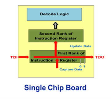
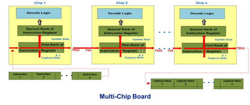
In the Part 4 blog, I described the process of loading the instruction register with an OPCODE. Once the instruction register is loaded with an OPCODE, an Update-IR takes place, which sends the OPCODE to the 2nd rank of the instruction register. The OPCODE is then decoded, and the instruction is executed. When the instruction is executed, one of the registers within the boundary scan device is configured between the TDI and TDO ports. In our example, the instruction OPCODE loaded into the instruction register was EXTEST. Once the instruction was decoded and executed, the register configured between the TDI and TDO ports was the boundary scan register. The process of loading instructions during boundary scan testing can take place on a printed circuit board with a single boundary scan device or on a printed circuit board with multiple boundary scan devices. During a sequence of boundary scan test actions, the boundary scan device may be instructed to execute EXTEST, IDCODE, BYPASS, etc. numerous times to accomplish the required boundary scan testing and programming objectives for the printed circuit board. Executing instructions require a scan down the Select-IR-Scan side of the TAP. The TMS and TCK ports of all boundary scan devices in the scan chain are connected in parallel, so their TAPs move in a synchronous fashion.
Let’s continue with our example and see what happens after the EXTEST instruction is loaded, decoded, and the boundary scan register is configured between the TDI and TDO ports.
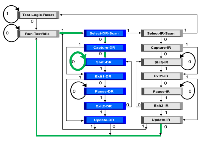
Step 4. TAP transitions to Run-Test/Idle and Select-DR-Scan
Referring back to the TAP state diagram and picking up at the Update-IR state, TMS goes to logic-0 then logic-1, which moves the TAP back to Run-Test/Idle then to Select-DR Scan. Note that Select-DR-Scan has the 3 major states of Capture, Shift, and Update as Select-IR-Scan.
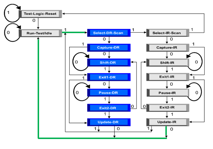
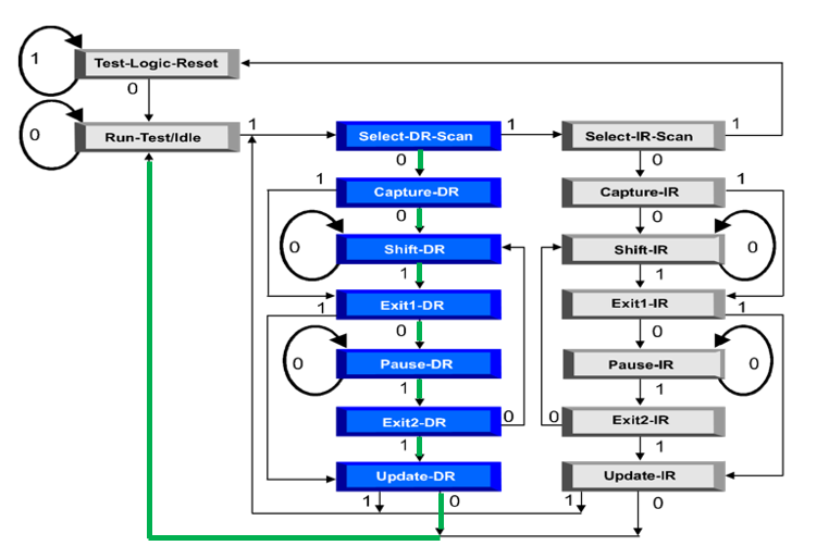
Step 5. TAP transitions to Capture-DR
TMS continues its transition on the rising edge of TCK to logic-0, which moves the TAP to Capture-DR.
Just as with the Capture-IR, parallel inputs of a register are observed. What parallel inputs are observed? Well, since the boundary scan register is configured between the TDI and TDO ports, it is the boundary scan register’s parallel inputs that will be observed. What exactly is the boundary scan register? I’ll explain what the boundary scan register is comprised of and its function.
The boundary scan register is used to transmit and receive test stimulus data for boundary scan devices. The boundary register is associated with the I/O pins of the device. Per 1149.1 every compliant boundary scan device has at least one boundary scan cell associated with one I/O pin. The boundary scan cell/pin association is listed in the BSDL in the attribute Boundary_Register section.
The boundary cell most often used for creating a boundary scan register is the BC_1 cell. The boundary scan register is a collection of boundary scan cells that are connected in a serial fashion, from serial input (SI) to serial output (SO), as pictured below. Boundary scan cells associated with input pins are called input cells, boundary scan cells associated with output cells are called output cells.
The boundary scan register, and the cell types that comprise it, are listed in the BSDL file. Below is a snippet of the BSDL describing the boundary scan register for our device KCSU1911. Cell numbers 1,2,4,5,7, and 8 are all BC_1. These cells are used for I/O control and output for pins IOG3, IOG2, and IOH1. Cell numbers 0,3, and 6 are BC_4 cells and are used for the device input for pins IOG3, IOG2, and IOH1. Another bit of information we see is the attribute Boundary_Length of KCSU1911 is that the boundary scan register is comprised 240 cells. We’ll explore the entire BSDL file and its attributes in a future blog.
Each boundary scan cell can capture observed data on its PI. Focusing on the input pin and input cell (shaded area) this observed data includes the initial state of the pin (either logic-0 or logic-1) and data sent to the input pin from an adjacent, connected device. The captured data can be shifted from its SO to the SI of the adjacent boundary scan cell. The captured data can be updated from its 1st rank to the 2nd rank of the cell and exposed to the system logic. Remember, all registers in boundary scan are double ranked. Let’s go a bit deeper into how the boundary scan cells are double ranked. If we “x-ray” the green blocks representing our boundary scan cells, we see that it is comprised of 4 logic elements.
There is a multiplexer (mux) device at PI which allows selection of 2 data paths, data from the PI (the device pin) or data from SI (the adjacent cell). A multiplexer, shortened to “mux” is a combinational logic circuit designed to switch one of several input lines through to a single common output line by the application of a control signal. The mux output between the two inputs is determined by the TAP when it is in the Shift-DR state. There is also a mux before the on-chip system logic which allows selection of 2 data paths, data from the PI (the device pin) or data from the output of a latch device, to pass to the system logic through PO. The mux between these two inputs is determined by the Mode selection line (whether the device is in boundary scan mode or normal functional mode). Latches are basic storage elements. The latches represent the 1st and 2nd rank of the cell. The 1st latch (1st rank) “stores” a single bit of data based on Clock-DR. It can send data via the SO path to the next adjacent cell. The 2nd latch (2nd rank) is controlled by the Update-DR. It can send data to the mux that controls what data enters the system logic.
Looking at the output cell associated with the output pin (shaded area), there are also 4 elements which comprise it. There is a mux at PI which allows selection of 2 data paths, data from PI (data from the system logic) or data from SI (the adjacent cell). The mux switch between the two inputs is determined by Shift-DR. There is also a mux before the device output pin which allows selection of 2 data paths, data from PI (data from the system logic) or data from a latch. The mux switch between these two inputs is determined by the Mode selection line (whether the device is in boundary scan mode or normal functional mode). The latch devices represent the 1st and 2nd rank of the cell. The 1st latch (1st rank) is controlled by the Clock-DR and the 2nd latch (2nd rank) is controlled by the Update-DR.
In summary the boundary scan cell can:
- Capture (parallel load) data on its parallel input PI
- Shift data from SO to its adjacent cell’s SI
- Update (parallel unload) data onto its parallel output PO
- Behave transparently (PI passes to PO) when the device is in normal operating mode
Because the cells can behave transparently, there is no performance impact to the device when in normal functional mode. This is a win-win scenario. Device manufacturers can implement boundary scan with the assurance that the functionality of their device won’t be degraded. Test engineers can choose boundary scan devices and take advantage of their inherent test capabilities.
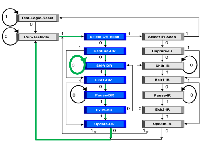
Step 6. TAP transitions to Shift-DR
TMS remains at logic-0 and the TAP enters Shift-DR. With a focus on the input side of the device, the mux is configured to allow the captured data from PI to pass through. The captured data from PI are shifted out of 1st rank. For the boundary scan register, the captured data is shifted to the adjacent input cell through SO. The TAP will remain in Shift-DR long enough to shift out the entire contents of the boundary scan register. Looking at the output side of the device, the same operation takes place. The mux is configured to allow the data from SI to pass through and into the 1st rank and to the adjacent output cell through SO. Our boundary scan device under examination has a total of 240 cells, so that means there will be 240 TCK cycles to shift out the captured data values from the 1st rank. The 240 bits of captured data values are shifted out of TDO and eventually back to ScanWorks. More on what happens with the captured data values will be covered in future blogs.
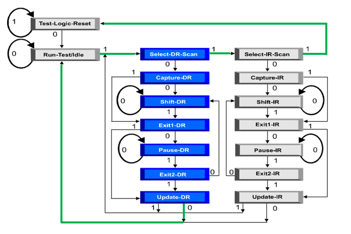
Step 7. TAP transitions to Update-DR and Run-Test/Idle
TMS transitions to Update-DR. At this state, data is updated from the 1st rank to the 2nd rank. Remember that for cells, update means sending data from the 1st latch to the 2nd latch. Focusing on the output cell, the Update-DR is particularly important. EXTEST activates the boundary scan register where inputs are observed. Those input data values are transmitted from other device outputs. ScanWorks receives values shifted back through the scan chain. These values are compared with data that ScanWorks expects. These expected data values can come from the BSDL when we are testing the instruction register. In the case of the boundary scan register, ScanWorks generates a set of data values to test for shorts and open nets. Without loading a known data value in the output cell, we would not know what data value to expect on the input side of the receiving input device. To accomplish this, an instruction is loaded prior to EXTEST, this instruction is PRELOAD. The PRELOAD instruction maintains the boundary scan device in its functional mode, while loading a known data value into the 1st rank of output cell. When the Update-DR stated is reached, the data value is sent to the 2nd rank then sent out the output.
Step 8. TAP Select-DR-Scan (multiple scans)
The EXTEST operation generates thousands of test patterns, so multiple Capture, Shift, and Updates may be performed until all the test patterns are exhausted.
Step 9. TAP exits Select-DR-Scan and return to Test-Logic-Reset
Once all boundary scan operations have been completed, the TAP returns to Test-Logic-Reset and the boundary scan device is returned to its functional mode.
There are a lot of operations that take place when executing boundary scan operations. Our boundary software ScanWorks handles all of these operations with the TAPs of the boundary scan devices responding to the TMS transitions initiated by ScanWorks on the rising edge of TCK. Boundary scan is a truly remarkable test technology. In the next blog, we’ll examine various cell configurations and the BSDL file for our device KCSU1911.