
In case you missed it, a recording of Michael Johnson’s webinar, Chiplet Interconnect Testing using JTAG/Boundary Scan, is now available. Click on the link, and enjoy the show.
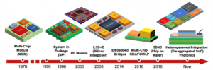
As the semiconductor industry continues to move toward more efficient and less expensive IC fabrication and design methodologies, an innovative packaging trend has emerged that was originally proposed during the 1960’s. This method proposed the packaging of multiple-die devices within a single IC package, a design method known as heterogenous integration.
Heterogenous integration involves the combination of diverse and separate elements, into a functional system. As applied to this use case, the diverse elements are silicon chips (herein referred to as chiplets); and when combined on an interposer or silicon substrate, constitute a structured functioning system.
These assembled, diverse silicon chiplets can be packaged in a variety of options of such as System on Chip (SoC), Multi-Chip Modules (MCM), System in a Package (SiP) and System on Package (SoP). There package methodologies consist of horizontally placed die (2.5D) and vertically stacking of chiplets (3D).
With this as background, the webinar covers the following agenda:
- Chiplet-based Multi-die Devices
- Moore’s Law – Extended
- Multi-die Device D2D Interconnects
- Testing Multi-die Device D2D Interconnects
- Standard Test Interface Language
- Using ScanWorks to Produce STIL
One question came up that I thought was particularly interesting, and deserved some follow-up: “Are Wagner patterns more stressful than Walking 1s/Walking 0s?”. This question came in the context of differentiating a fairly easy-to-implement “walking pattern” algorithm for doing structural testing, versus the Wagner vector-based approach. I wanted to add that Wagner is more compact (dense) in terms of pattern generation and defect diagnostics; further, Wagner patterns provide more interconnect activity on each test cycle than walking 1s/0s (you can often get walking 1s/0s from your EDA provider, if using embedded boundary scan), thus stressing the power distribution network somewhat (think in terms of simultaneous switching); so Wagner might pick up some marginalities that walking 1s/0s miss.
Check out the video here (note: requires registration). Hope you find it interesting.