
DDR4 SDRAM brings lower voltage and faster speeds. What are the implications for system marginality validation (SMV)?
DDR4 SDRAM is an evolutionary technology, compared to DDR3. Among the many improvements/ changes are:
- Increase in data rate – typically from 2,133 MT/s up to 3,200 MT/s
- Reduction in power – from 1.5V down to 1.2V
- On-die termination (ODT) has an additional RTT_PARK “parked” value, adding to RTT_NOM and RTT_WR values
- Data bus inversion (DBI) which reduces power consumption and simultaneous switching output (SSO), thereby improving signal integrity
- CMD/ADDR parity
- Write CRC
- VREFDQ is now internal – as opposed to on DDR3, where VREFDQ is via on-board circuitry
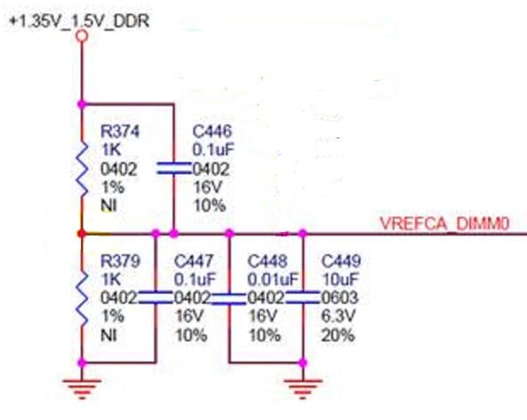
Let’s examine the last item in some detail. Most board designs which are capable of having their DDR3 VREFDQ margined do so via an external circuit, which might look something like this:

The circuit is controlled in turn by a digitally (i.e. I2C) controlled potentiometer, such as the Intersil ISL90727, that allows the VREFDQ to be derived from the main supply.
Whereas with DDR4, VREFDQ is generated on-die, which reduces board cost and routing area. What this means, is that the DDR4 memory internal VREFDQ must be varied under control of the memory controller. The DRAM controller manages the on-die VREFDQ through a programmable configuration register (in this case, mode register 6 (MR6), bits 7:0) which resides in the DRAM.
It is worthwhile noting that with the high speeds specified for DDR4, the actual center of the data eye provided to the DRAM may shift up and down slightly from one device to another. This could be due to variances in PCB layout, power distribution SSO, temperature, or other effects. During initialization of the DDR4 bus, the controller communicates with the DRAM to discover the optimal VREFDQ setting for each DRAM to minimize the error rate. This can differ from device to device so per-DRAM addressability (PDA) is provided. This happens during VREFDQ training. Note also that on-die termination (ODT) and drive strength, which play key roles in the DRAM signal integrity, can be set at initialization /training, and periodically recalibrated.
As can be seen, DDR4 memory has several features which inherently improve signal integrity. These are necessary in light of its higher speeds and lower voltages. But for DDR4, CMD/ADDR is becoming more of a margin limiter. Further, the DDR4 spec defines the data-valid window in terms of a BER of 1E-16 (as a parallel bus this is more stringent than, say, PCI Express Gen3 at 1E-12 or Intel QuickPath Interconnect (QPI) at 1E-14), rather than a static tDS/tDH. And, if you want to improve the reliability to a smaller BER such as 1E-18 (a failure every two weeks), or 1E-20 (a failure every four years), you have to open the eye much further. All this points to the importance of system marginality validation (SMV), which is described in further detail here in the blog, Signal Integrity Validation (SIV) versus System Marginality Validation (SMV) – Part 3.
For more information on validating and testing memory, a good resource is our eBook, Testing High-Speed Memory with Embedded Instruments.
2 Responses
Thanks, Alan, for keeping us informed, as always! Clearly, system margin validation (SMV), for obvious reasons, I suppose, continues to become more and more important as per-line transfer rates continue to climb.
Here are just a couple of comments by way of clarification – I hope they are of help!
• Regarding the circuit snip and the reference to the digital potentiometer – if the ISL90727 is used, for the stated purpose of margining the VREF, then the 1K resistors become NI (not installed) and the three (3) resistance terminals (RH, RW and RL) connect in their place (at the VDDQ, VREF and GND, respectively).
• Near the end, you say that, “But for DDR4, CMD/ADDR is becoming more of a margin limiter.” To be clear, I believe that the referent for the “more” (than) here is CMD/ADDR for DDR3 (rather than, for example, DQ for DDR4 itself).
My pleasure, Adam.
You are absolutely correct regarding the circuit snip.
And yes, both DQ and CMD/ADDR are margin limiters, but more attention must be paid to CMD/ADDR margining on DDR4. Design engineers usually focus on DQ voltage and timing margining as part of design validation, and ignore CMD/ADDR margining, but this is no longer practical for DDR4.