We know from empirical evidence that a system’s operating
margins are as sensitive to the chips on the board, as they are to the board’s
design and manufacturing process itself. Why is this so?
See how Margins (Eye Diagrams) follow the Silicon in the white paper Platform Validation Using Intel® Interconnect Built-In Self Test (Intel® IBIST) from DesignCon. In this white paper, we demonstrated empirical evidence that showed that a system’s
overall signal integrity is quite sensitive to the chips themselves. So if you
test the same board design numerous times with different chips, you’ll get
swings in the size and shape of the eye diagrams for high-speed SerDes I/O and
memory. Obviously, there are sources of variances within the chip production
itself, going from wafer to die, especially as it concerns process variation
and leakage as dies shrink (i.e. going from 45nm to 32nm to 22nm and so on).
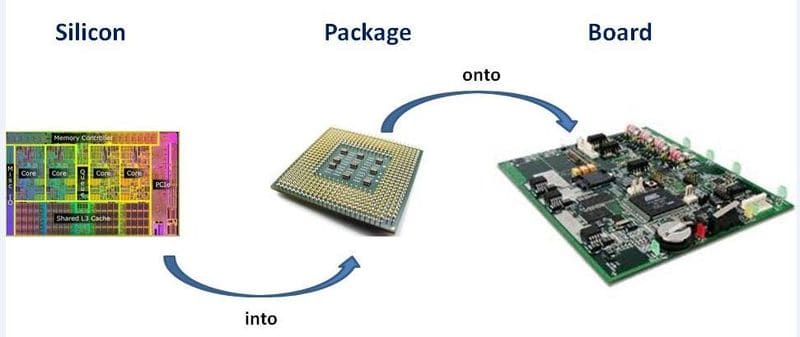
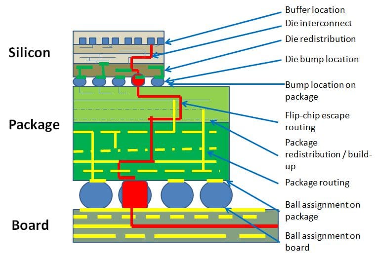
This is due to chip design being very analogous to board
design, but on a nano-geometry level. It’s easiest to see this analogy
visually:
So, given the complexity of I/O floorplanning, logic
synthesis, placement, clock insertion, routing, timing closure, manufacturing and
so on, it’s not surprising that margins vary from chip to chip.
Add that to the variances introduced from board to board,
and it’s easy to see that a typical signal integrity validation cycle might involve at a minimum 5 tests on 5 systems (also known as a 5X5 procedure). For more information on a typical validation
methodology using this approach, see our application brief here.


