
In the world of medical device manufacturing, there is no margin for error. The electronic systems at the heart of diagnostic imagers, patient monitors, and life-support equipment are governed by a mandate for perfection. A single faulty solder joint or a microscopic flaw in a circuit is not merely a quality issue; it is a potential threat to patient safety. This high-stakes environment has zero tolerance for “blind spots,” areas on a complex Printed Circuit Board (PCB) where manufacturing defects can hide from conventional test methods, creating uncontrolled risks.
As medical devices become more powerful and compact, their underlying electronics grow exponentially more complex. For an engineering director, this presents a dual challenge: how do you accelerate time-to-market while ensuring the absolute, verifiable integrity of every board, especially when managing multiple manufacturing sites or third-party suppliers? The answer lies in a diagnostic strategy that provides a granular, unambiguous view of a PCB’s structural health, leaving no room for doubt.
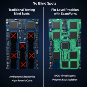
The Challenge of the Invisible Fault
For decades, testing assembled PCBs relied on the “in-circuit test” (ICT) method, which uses a “bed-of-nails” fixture with physical probes to make contact with the board. This approach is no longer viable. Two key trends have made physical access a relic of the past:
- Advanced Component Packaging: High-density packages like Ball-Grid Array (BGA) have their electrical connections, an array of solder balls, hidden underneath the chip. Once soldered to the board, these connections are completely inaccessible to physical probes.
- Multi-Layer Boards: To support modern design density, critical connections are often routed on internal layers buried deep within the PCB, physically unreachable from the surface.
This irreversible loss of physical access creates a critical gap in quality assurance. It becomes impossible to physically verify that the manufactured board matches the original design schematic. For an industry governed by standards like ISO 13485, which mandates rigorous design verification and process validation, this is a significant compliance risk.
Lighting Up the Board: Virtual Access with Boundary-Scan
In response to this challenge, the industry developed the IEEE 1149.1 standard, commonly known as boundary-scan or JTAG. This elegant architecture builds testability directly into the silicon of the integrated circuits (ICs) themselves.
Boundary-scan works by embedding a chain of memory elements, or “cells,” at the boundary of each compliant chip, between its internal logic and its external pins. On a board, the chains of multiple devices are linked together, creating a single, board-wide electronic test path. This path is controlled through a simple, standardized interface called the Test Access Port (TAP).
A test system like the ASSET® ScanWorks® platform uses this virtual path to electronically control and observe the state of every pin on the chain, creating “virtual nails” with 100% access. This allows for comprehensive testing of manufacturing defects like open circuits and shorts without ever touching the board with a physical probe.
A Multi-Layered Diagnostic Strategy with ScanWorks
A robust test strategy is a layered, methodical process. ScanWorks embodies this philosophy by providing a suite of targeted actions that systematically verify a board’s integrity, ensuring that when a fault is found, it is isolated with precision.
Step 1: Verifying the Test Infrastructure (Scan Path Verify)
Before testing the board, you must first ensure the testing mechanism functions correctly. The ScanWorks Scan Path Verify (SPV) action validates the integrity of the boundary-scan infrastructure itself. It confirms the TAP controllers are working and the scan chain is intact. In ScanWorks training exercises, when a fault is introduced into the chain, the SPV action and its interactive debugger allow an engineer to instantly pinpoint the exact location of the break. This ensures the test itself is trustworthy.
Step 2: Finding Manufacturing Defects (Interconnect Test)
The Interconnect action is the workhorse for detecting opens, shorts, and stuck-at faults between components. When a test fails, ScanWorks generates a detailed Pin Level Diagnostic Report that identifies the fault type, the specific nets involved, and the exact device pins connected to the fault. Furthermore, an engineer can click on a failing pin and the ScanWorks Design Browser will highlight its physical location on the board’s layout, transforming abstract data into an actionable repair location.
Step 3: Securing Complex Interfaces (Memory & Flash Tests)
Modern devices rely on complex peripheral components like RAM and Flash memory. The ScanWorks Memory Access Verify (MAV) and Flash actions are designed to test the structural integrity of these critical interfaces. The MAV action tests the data, address, and control lines to memory, isolating faults down to the specific net. Similarly, the Flash action’s “Interactive Programmer” can perform a “Walking One Test” to verify every connection to a Flash device, providing clear diagnostic results if a fault is found.
This comprehensive approach ensures no blind spots exist, even on the high-speed, high-pin-count interfaces common in today’s advanced medical electronics.
| Fault Type | Description | ScanWorks Action | Key Diagnostic Tool / Report |
| Scan Chain Integrity | An open/short in the JTAG path or an incorrect device ID. | Scan Path Verify (SPV) | Run Log, Interactive Debugger |
| Interconnect Fault | An open, short, or stuck-at fault on a net between components. | Interconnect | Pin Level Diagnostic Report, Design Browser |
| Memory Interface Fault | A fault on an address or data bus connected to a RAM device. | Memory Access Verify (MAV) | Memory Diagnostic Report, Interactive Debugger |
| Flash Interface Fault | A fault on the connections to a Flash memory device. | Flash | Interactive Programmer (e.g., Walking One Test) |
Beyond Diagnostics: Forging an Audit-Proof Trail
For medical device manufacturers, technical capability is only half the battle. The true value of ScanWorks is its ability to transform the testing process into a powerful compliance asset. The detailed, structured data generated by ScanWorks provides the objective evidence demanded by ISO 13485.
The reports generated by ScanWorks are permanent, auditable records. Each test run can be linkedis linked to a unique UUT serial number, is time-stamped, and contains a complete record of the actions performed and their outcomes. This provides the unambiguous, granular traceability auditors require. A passing interconnect test from ScanWorks is documented proof that the board was manufactured as designed, fulfilling Design Verification mandates. When process validation is required for steps like BGA soldering, where the output cannot be fully inspected, ScanWorks data provides the objective evidence that the process is consistently producing compliant products.
This data inherently aligns with the principles of ALCOA+ (Attributable, Legible, Contemporaneous, Original, Accurate, and Complete), a framework that defines the characteristics of trustworthy data for regulatory environments.
| ALCOA+ Principle | How ScanWorks Delivers |
| Attributable | Reports are time-stamped and can be linked to a UUT serial number and test station. |
| Legible | Reports are generated in standard, human-readable formats (HTML, Text) and stored electronically. |
| Contemporaneous | Test logs are generated in real-time as the test sequence executes. |
| Original | The electronic report is the primary, original output from the test instrument. |
| Accurate | The data represents the direct, unaltered measurement from the hardware. |
| Complete | Diagnostic reports include all relevant information: failing nets, pins, expected vs. measured data, and context. |
Conclusion: From Diagnostic Precision to Patient Safety
The loss of physical test access has created the potential for dangerous blind spots in the manufacturing of medical electronics. Boundary-scan technology, as implemented by the ScanWorks platform, restores 100% test access and provides the pin-level diagnostic precision needed to eliminate these risks.
ScanWorks bridges the gap between technical execution and regulatory obligation. Its capabilities do more than just find faults; they generate a rich, detailed, and auditable dataset that directly supports the core tenets of ISO 13485. By empowering engineering leaders with the tools to see everything, test everything, and document everything, ScanWorks delivers the confidence needed to ensure every device is not only functional, but verifiably safe, effective, and compliant.
With the diagnostic confidence and compliance capabilities of ScanWorks established, the strategic question turns to implementation. As many teams re-evaluate the high costs and time delays of traditional PCB testing outsourcing, discover the advantages of an in-house approach in our companion article: Why Healthcare Engineering Teams Are Reconsidering PCB Testing Outsourcing | ASSET InterTech.