Today, February 15th, 2020, marks the official 30th Anniversary of JTAG. What a wild ride it has been – from its humble beginnings for detecting short and open circuits, it has evolved to be, in some ways, the most powerful and feared technology on the planet. How did we get here?
On February 15th, 1990, the IEEE Standard Board ratified the 1149.1-1990 – IEEE Standard Test Access Port and Boundary-Scan Architecture. IEEE 1149.1, also known as “JTAG” for the Joint Test Action Group that created it, is the specification that became the foundation of many other in-chip related technologies, such as:
1149.6 – IEEE Standard for Boundary-Scan Testing of Advanced Digital Networks
1532 – IEEE Standard for In-System Configuration of Programmable Devices
1149.7 – IEEE Standard for Reduced-Pin and Enhanced-Functionality Test Access Port and Boundary-Scan Architecture
1687 – IEEE Standard for Access and Control of Instrumentation Embedded within a Semiconductor Device
1838 – IEEE Approved Draft Standard for Test Access Architecture for Three-Dimensional Stacked Integrated Circuits
and many more.
The amazing thing about JTAG is, over the last 30 years, it has become instantiated in almost all commercial silicon of any complexity. That, in and of itself, makes it a technology that is subject to a lot of interest. But, in many ways, it is widely misunderstood, and therefore sometimes an object of trepidation. What is it about the architecture that makes it so powerful and feared?
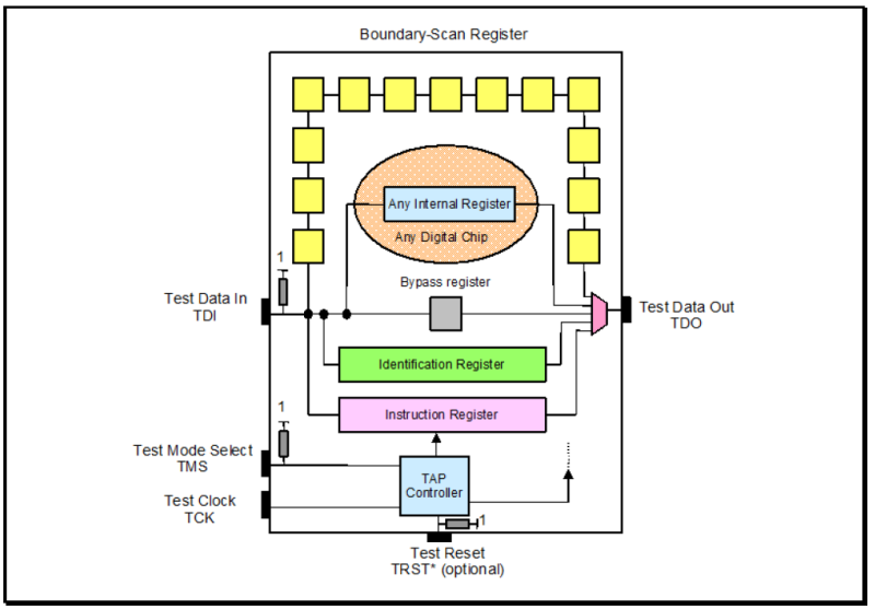
A stylized diagram of a chip with JTAG in it is below:
The architecture has the following main components:
A set of four dedicated test pins — Test Data In (TDI), Test Mode Select (TMS), Test Clock (TCK), Test Data Out (TDO) — and one optional test pin Test Reset (TRST*). These pins are collectively referred to as the Test Access Port (TAP).
A boundary-scan cell on each pin, connected internally to form a serial boundary-scan register.
A finite-state machine TAP controller with inputs TCK, TMS, and TRST*.
An n-bit (n >= 2) Instruction register, holding the current instruction.
A 1-bit Bypass register.
An optional 32-bit Identification register capable of being loaded with a permanent device identification code.
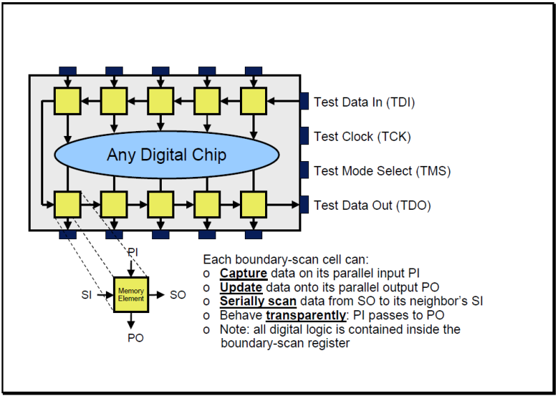
And a closer look at one of the boundary-scan cells, that make up the boundary register, is below:
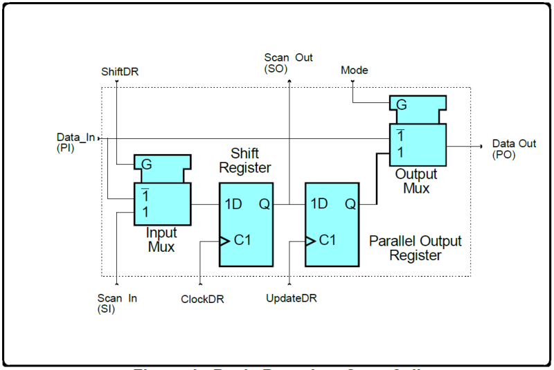
Look at this carefully: this is why JTAG is sometimes feared. There is some JTAG logic behind each pin, a boundary scan cell, that can not only shift data serially around the perimeter of the device, but also shift data between the pins interfacing to the outside world and the internal system logic. And, as an example of a boundary scan cell, consider the following:
This example boundary scan cell has four modes of operation: Normal, Update, Capture, and Serial Shift. The memory element is a simple D-type flip-flop with front-end and back-end multiplexing of data.
During Normal mode, PI is passed transparently straight through to PO. In other words, JTAG sits in the background and does essentially nothing.
During Update mode, the content of the output register is passed through to PO. Data is sent to the outside world.
During Capture mode, the PI signal is routed to the shift register and the value is captured on the next ClockDR.
During Serial Shift mode, the SO of one register flip-flop is passed to the SI of the next via a hard-wired path.
Note that both Capture and Serial Shift operations do not interfere with the normal passing of data from the parallel-in (PI) terminal to the parallel-out (PO) terminal. This allows, at least in theory, the capture of operational values “on the fly” and the movement of these values for inspection without interference with functional modes of operation.
Capturing system logic data, transparently shifting data along the periphery of the device, sending traffic out of the device in a bare metal, out-of-band way….powerful, huh?
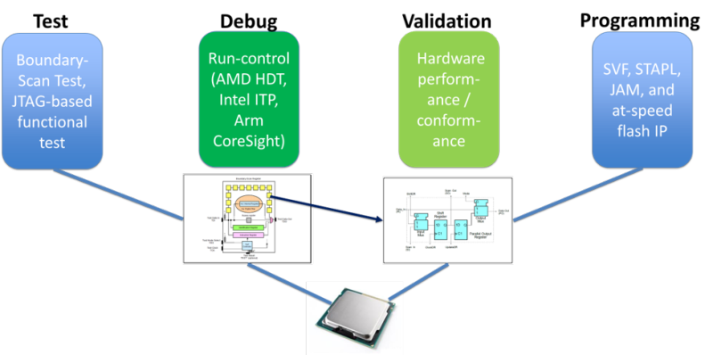
With such simple, elegant logic present in most chips, over the years four major application areas have grown up around JTAG, as shown in the following diagram:
Let’s look at these areas in some detail; you can skip this section if you’re familiar with them.
Test
For test, JTAG provides the support infrastructure for boundary-scan test (BST), and is used for PCB structural test, typically in a manufacturing production context. The boundary scan architecture provides a means to test interconnects (including clusters of logic, memories, etc.) without using physical test probes; this involves the addition of at least one test cell that is connected to each pin of the device and that can selectively override the functionality of that pin. Each test cell may be programmed via the JTAG scan chain to drive a signal onto a pin and thus across an individual trace on the board; the cell at the destination of the board trace can then be read, verifying that the board trace properly connects the two pins. In this instance, an optimal set of test patterns (vectors) are created, using for example the Wagner algorithm, to optimize defect detection and isolation, based upon the board design. These patterns are scanned out on the stimulus side and read on the response side in sync with TCK, looking for mismatches and identifying, where possible, the nets/pins that are at fault.
JTAG also provides the support technology for out-of-band at-speed functional test on CPU-based designs. One approach is to use JTAG to scan small test programs into CPU On-Chip Memory (OCM). This eliminates the need for board system memory, or even any other board critical functions other than the CPU itself, to be initialized prior to executing the test program. The CPU then executes the test program at CPU speeds (instead of via a slow TCK-based “static” test), treating its own cache as RAM, and the results are retrieved back to the test program via JTAG. This is often much faster than boundary scan-based functional test.
Device Programming
Boundary scan can also be used to program devices using the Serial Vector Format (SVF), a textual representation of JTAG operations using a simple syntax. Other programming formats include 'JAM', ‘STAPL’ and the more recent IEEE Std. 1532 In-System Configuration ('ISC'). Files in these formats contain higher-level instructions whose purpose is to manage the needed JTAG state machine transitions, and stream the needed image data out the boundary scan cells. Using JTAG, flash memories, FPGAs, CPLDs, microcontrollers embedded flash, and I2C, SPI and PMBus serial devices can be programmed via their own JTAG interfaces, or via surrounding JTAG devices.
As with Test, Programming using JTAG can also be performed by using a functional approach, as opposed to wiggling the boundary scan cells. Dedicated programming IP can be loaded into CPU cache or FPGA logic, and then executed to load images and data in at-speed. This results in much higher performance, with the commensurate cost savings.
Using JTAG has the benefit of programming devices after they have been mounted on the board, and permits easy in-situ reprogramming for product field upgrades.
Debug
Today, one of the primary applications of JTAG is for accessing logical sub-blocks within integrated circuits dedicated to what is commonly called “run-control”. These logic blocks provide an essential mechanism for debugging embedded systems that may not have any other debug-capable communications channel. On many systems, JTAG-based debugging is available from the very first instruction after CPU reset, allowing it to assist with development of early boot software that runs before any device or bus is initialized.
In this use case, a hardware emulator or probe uses JTAG as the transport mechanism to access on-chip debug modules inside the target CPU. Those modules let software developers debug the software of an embedded system directly at the machine instruction level when needed, or (more typically) in terms of high-level language source code. Many silicon architectures such as PowerPC, MIPS, Arm, and x86 have built an entire software debug, instruction tracing, and even data tracing infrastructure around the basic JTAG protocol. Some examples are Arm CoreSight, Intel Last Branch Record (LBR) and Intel Processor Trace (IPT).
With JTAG-based run-control, processors can be halted, single-stepped, or let run freely. System registers, memory, and I/O buses can be read and written to. One can set code breakpoints, both for code in RAM and in ROM/flash memory. Some CPUs support only "halt mode debugging", but others allow debuggers to access registers and data buses without requiring cores to be halted.
Validation
In the context of JTAG, Validation as a use case often uses the same run-control capabilities as described in the description of Debug above. The ability to read/write platform registers, memory and I/O presents the ability to extract platform “golden states” and compare these against a best-known configuration. This can validate if a platform is in the desired state at the end of boot flow initialization, by examining register contents and comparing them against what was supposed to be set by the bootloader. Low-level firmware and driver bugs can be identified in this way.
Further, run-control can be used to exercise system devices, buses and memory using JTAG as an out-of-band engine, obviating the need to boot systems prior to test. In some cases, JTAG access to low-level register reads/write mechanisms within silicon yield a much faster validation cycle.
Finally, JTAG can use its register/ memory/ IO “write” capability to perform error injection on such buses, to see how they behave under failure conditions. One example of this is to induce different types of bit errors on memory, stressing the memory controller's error handling ability, and seeing that the system does (or does not) recover from corrrectable and uncorrectable faults.
If you’re still with me at this point, you can see that JTAG is an enormously useful technology. It’s very mature, with 30 years of deployment, and runs quietly in the background within billions of devices. Without it, we would need to find other means to debug, test, validate and program our electronics systems – mostly likely using physically intrusive “bed of nails” systems, where that might even be possible – adding untold cost, both from a monetary and a planetary ecosystem impact standpoint.
But, with great power comes great responsibility. Could JTAG be used for side-channel attacks? If you’d like to read more on this topic, I’d suggest my Securing the JTAG Interface blog.


