JTAG is coming up on its 30th anniversary. And some would say it’s older than that. As I prepared for doing an introductory presentation on this amazing technology, I got a chance to reflect on how useful it has become, and what the next 30 years might be like.
JTAG came about in the mid-1980s when a group of concerned test engineers in a number of European electronics systems companies got together to examine the problem of board test access. With increasing design and complexity, it was foreseen that traditional “bed-of-nail” test access was coming to the end of the line. A group of engineers initially calling themselves the Joint European Test Action Group (JETAG) got together to collaboratively address the problem:
Later, the group was joined by representatives from North American companies, and the ‘E’ for “European” was dropped from its, leaving it as “Joint Test Action Group”, or JTAG.
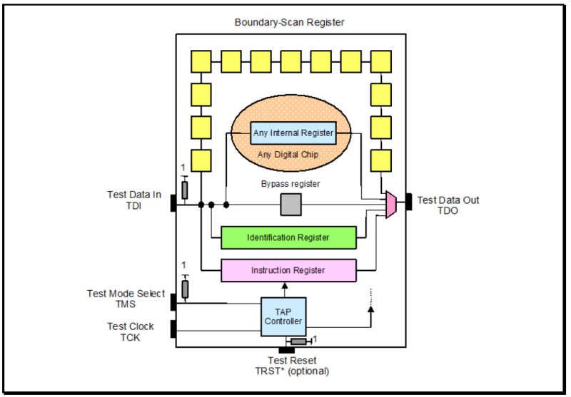
The group’s preferred solution involved restoring the access to device pins by means of an internal serial shift register around the boundary of the device – what was in essence a boundary scan register – combined with a state machine:
As you can see, the diagram describes the implementation’s elements:
- A set of four dedicated test pins — Test Data In (TDI), Test Mode Select (TMS), Test Clock (TCK), Test Data Out (TDO) — and one optional test pin Test Reset (TRST*). These pins are collectively referred to as the Test Access Port (TAP).
- A boundary-scan cell on each device primary input and primary output pin, connected internally to form a serial boundary-scan register (Boundary Scan).
- A finite-state machine TAP controller with inputs TCK, TMS, and TRST*.
- An n-bit (n >= 2) Instruction register, holding the current instruction.
- A 1-bit Bypass register (Bypass).
- An optional 32-bit Identification register capable of being loaded with a permanent device identification code.
The amazing thing about JTAG is that, with this little bit of logic built into almost all commercial silicon, powerful use cases have evolved to encompass almost all aspects of electronics board and system lifecycles. These fall into four main areas:
- Test
- Device Programming
- Debug
- Validation
Let’s look at these briefly.
Test
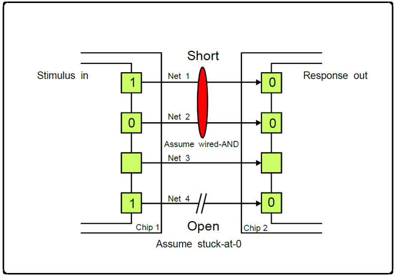
For test, JTAG provides the support infrastructure for boundary-scan test (BST), and is used for PCB structural test, typically in a manufacturing production context. The boundary scan architecture provides a means to test interconnects (including clusters of logic, memories, etc.) without using physical test probes; this involves the addition of at least one test cell that is connected to each pin of the device and that can selectively override the functionality of that pin. Each test cell may be programmed via the JTAG scan chain to drive a signal onto a pin and thus across an individual trace on the board; the cell at the destination of the board trace can then be read, verifying that the board trace properly connects the two pins. Here are a couple of examples:
An optimal set of test patterns (vectors) are created, using for example the Wagner algorithm, to optimize defect detection and isolation, based upon the board design. These patterns are scanned out on the stimulus side and read on the response side in sync with TCK, looking for mismatches and identifying, where possible, the nets/pins that are at fault.
JTAG also provides the support technology for out-of-band at-speed functional test on CPU-based designs. One approach is to use JTAG to scan small test programs into CPU On-Chip Memory (OCM). This eliminates the need for board system memory, or even any other board critical functions other than the CPU itself, to be initialized prior to executing the test program. The CPU then executes the test program at CPU speeds (instead of via a slow TCK-based “static” test), treating its own cache as RAM, and the results are retrieved back to the test program via JTAG. This is often much faster than boundary scan-based functional test.
Device Programming
Boundary scan can also be used to program devices using the Serial Vector Format (SVF), a textual representation of JTAG operations using a simple syntax. Other programming formats include ‘JAM’, ‘STAPL’ and the more recent IEEE Std. 1532 In-System Configuration (‘ISC’). Files in these formats contain higher-level instructions whose purpose is to manage the needed JTAG state machine transitions, and stream the needed image data out the boundary scan cells. Using JTAG, flash memories, FPGAs, CPLDs, microcontrollers embedded flash, and I2C, SPI and PMBus serial devices can be programmed via their own JTAG interfaces, or via surrounding JTAG devices.
As with Test, Programming using JTAG can also be performed by using a functional approach, as opposed to wiggling the boundary scan cells. Dedicated programming IP can be loaded into CPU cache or FPGA logic, and then executed to load images and data in at-speed. This results in much higher performance, with the commensurate cost savings.
Using JTAG has the benefit of programming devices after they have been mounted on the board, and permits easy in-situ reprogramming for product field upgrades.
Debug
Today, one of the primary applications of JTAG is for accessing logical sub-blocks within integrated circuits dedicated to what is commonly called “run-control”. These logic blocks provide an essential mechanism for debugging embedded systems that may not have any other debug-capable communications channel. On many systems, JTAG-based debugging is available from the very first instruction after CPU reset, allowing it to assist with development of early boot software that runs before any device or bus is initialized.
In this use case, a hardware emulator or probe uses JTAG as the transport mechanism to access on-chip debug modules inside the target CPU. Those modules let software developers debug the software of an embedded system directly at the machine instruction level when needed, or (more typically) in terms of high-level language source code. Many silicon architectures such as PowerPC, MIPS, Arm, and x86 have built an entire software debug, instruction tracing, and even data tracing infrastructure around the basic JTAG protocol. Some examples are Arm CoreSight, Intel Last Branch Record (LBR) and Intel Processor Trace (IPT).
With JTAG-based run-control, processors can be halted, single-stepped, or let run freely. System registers, memory, and I/O buses can be read and written to. One can set code breakpoints, both for code in RAM and in ROM/flash memory. Some CPUs support only “halt mode debugging”, but others allow debuggers to access registers and data buses without requiring cores to be halted.
Validation
In the context of JTAG, Validation as a use case often uses the same run-control capabilities as described in the description of Debug above. The ability to read/write platform registers, memory and I/O presents the ability to extract platform “golden states” and compare these against a best-known configuration. This can validate if a platform is in the desired state at the end of boot flow initialization, by examining register contents and comparing them against what was supposed to be set by the bootloader. Low-level firmware and driver bugs can be identified in this way.
Further, run-control can be used to exercise system devices, buses and memory using JTAG as an out-of-band engine, obviating the need to boot systems prior to test. In some cases, JTAG access to low-level register reads/write mechanisms within silicon yield a much faster validation cycle.
Finally, JTAG can use its register/ memory/ IO “write” capability to perform error injection on such buses, to see how they behave under failure conditions. One example of this is to induce different types of bit errors on memory, stressing the memory controller’s error handling ability, and seeing that the system recovers (or does not recover) from correctable and uncorrectable faults.
Not bad for 30 years, huh? And what’s left for the next 30 years? Well, it’s pretty clear that the technology will continue to be going strong for at least that long, simply because there’s no alternative to it. With deployment in billions and billions of devices across the globe, over a period of decades, it will continue to prove its efficacy for years to come. So, it will continue to be used for test, device programming, debug and platform validation. But, there are new applications coming. I’ll write more about them next time!
As a hint, one novel new approach for enhancing platform diagnostics using JTAG as a proven, mature technology is in the form of Built-In Test. For more information, check out our eBook at Embedded JTAG for Boundary-Scan Test.


