In previous blogs, we contrasted the use of oscilloscopes to perform signal integrity validation (SIV) against silicon embedded instruments for system marginality validation (SMV). Why is SMV superior?
Signal integrity validation (SIV) uses oscilloscope measurements of select voltage and timing parameters across certain process/voltage/temperature (PVT) corner conditions and interface configurations. The intent of SIV is to ascertain transmitter and link robustness via oscilloscope waveform captures. The problem with SIV is that it is expensive, difficult, and slow. Oscilloscopes are extremely costly, getting access to the required buses can take weeks and may even be impossible, and typically the limited number of channels means that signal integrity issues can easily escape detection.
System marginality validation (SMV), on the other hand, uses embedded instrumentation within silicon to perform system level margining using I/O buffer control knobs such as VREF, buffer strength, slew rate, and timing controls, with Process/Voltage/Temperature (PVT) and interface configuration variability “baked in” to an eye mask that defines an acceptable margin. SMV proves in the entire system robustness, including transmitter, receiver, and interconnect link.
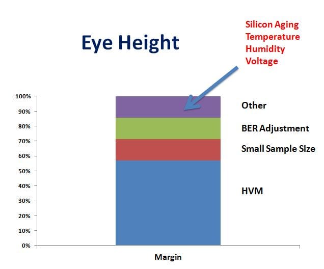
By margining the entire system, SMV provides a level of confidence in its overall performance. Further, when done properly, the eye mask takes into consideration chip design and manufacturing statistical variances which can cause the device to degrade over time. This can be shown visually:
High Volume Manufacturing (HVM) refers to the fact that variances occur within devices’ manufacturing processes which cause their own internal signal integrity to vary within and between lots. The effect of these variances is typically Gaussian in distribution.
Small Sample Size refers to the fact that SMV is often run on a finite number of samples. For example, as part of a 5×5 methodology (five SMV tests done across five different boards), five different chips are used as part of the validation testing. The effects of variances within the chips requires that a statistically large-enough sample size is needed for measurements. A single measurement is insufficient, and the larger the sample size, the higher the confidence. As an example of this, Altera[i] has created an extensive database of customer backplanes to calibrate their eye mask and refine their on-chip equalization schemes.
BER Adjustment takes into account that a bit error rate (BER) measurement is made at each margining point to detect correctable or uncorrectable faults. Given that, for example, the acceptable bit error rate threshold of Intel QuickPath Interconnect is 1 X 10E14, an extremely long period of time (in the hours or days) would be needed at each margining point (defined voltage and timing step) to detect such errors. The BER Adjustment extrapolates the error rate based upon a very short measurement time – typically less than a second.
The Other category represents adjustments to the eye mask made for silicon aging, humidity, pollution, process/voltage/temperature (PVT), and other factors.
SMV has emerged as a viable means of measuring the margin of systems within real world environments. As a methodology, it has been adopted widely within the semiconductor community by companies such as Intel, PLX, Altera, Xilinx, Broadcom, TI and others. Oscilloscopes are still needed, at least in the early stages of product development, for compliance testing and for SIV. But SMV is the preferred means of determining how much margin is in the design.
More information on the nature of chip and board defects and variances which affect system margins is in our tutorial, Detection and Diagnosis of Printed Circuit Board Defects and Variances using on-chip embedded instrumentation.


