Boundary scan is known to be quite slow to program large flash devices. But, with a new approach using SPI Master IP within an FPGA, flash programming time can be decreased by a factor of 15 or more.
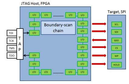
In the traditional approach where, for example, a SPI flash is connected to an FPGA, data is scanned through the FPGA internal chain and output to the targeted SPI device.

The speed of this method is typically limited by the size of the FPGA’s boundary register, which can be greater than 1,000 cells.
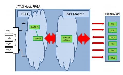
A better method involves having a SPI Master programmed into the FPGA using an IJTAG infrastructure, with a FIFO memory area whose size complements the page sizes of the SPI memory device. A cleverly designed SPI Master IP and a high-throughput boundary-scan controller are typically able to reach the maximum programming speed of the SPI memory device.
One customer saved over $262K per year using this approach:
Production run rate = 50,000 units/year
Cost of programming time on tester = $0.68/minute = $0.011/second
Programming time using short chain approach = 507 seconds
Programming time using FPGA IP approach = 30 seconds
Savings = 50,000 units/year X (507 – 30 seconds/unit) X $0.011/second = $262,350/year.
More information on this methodology is in the white paper At-Speed SPI Flash/EEPROM Programming Using FPGA and JTAG.


