In the blog Boundary-Scan Testing of PCI Express, we examined how JTAG
can be used to detect structural defects on high-speed serial I/O. Now let’s
review the situation for DDR3 and DDR4 memory.
In my blogs Defects on High-Speed Memory and Defects on High-Speed
Memory – Part 2, I covered
how important it is to detect structural defects on memory nets. Some shorts and
opens (such as a DQ stuck high or open) will cause a memory channel to be
mapped out or even a catastrophic error; other defects (such as two DQ shorted
together, or a DQS stuck at GND) may be invisible to conventional functional
test, but may cause high error counts and memory performance issues after the
product is shipped.
So, as we did with
the PCI Express case study, let’s examine some extracts of a hypothetical BSDL
of a commercially-available processor, and look at the boundary register cell
definitions for some of the memory nets:
"271 (BC_0, *,
control, 1 ),"
&
"272 (BC_0, DDR3_DQS_DN_16, output3, x, 271, 1, z ),"
&
"273 (BC_8, DDR3_DQ_63, bidir, x, 271, 1, z ),"
&
"274 (BC_8, DDR3_DQ_62, bidir, x, 271, 1, z ),"
&
.
.
.
"335 (BC_0,
DDR3_MA_10, output3, x,
271, 1,
z )," &
"336 (BC_0,
DDR3_CAS_N, output3, x,
271, 1,
z )," &
"337 (BC_0,
DDR3_RAS_N, output3, x,
271, 1,
z )," &
"338 (BC_0,
DDR3_WE_N, output3, x,
271, 1,
z )," &
"339 (BC_0,
DDR3_BA_0, output3, x,
271, 1,
z )," &
"340 (BC_0,
DDR3_BA_1, output3, x,
271, 1,
z )," &
"341 (BC_0,
DDR3_MA_0, output3, x,
271, 1,
z )," &
"342 (BC_0,
DDR3_MA_PAR, output3, x,
271, 1,
z )," &
.
.
.
"348 (AC_1,
DDR3_CLK_DP_0, output3, x,
271, 1,
z )," &
"349 (AC_1,
DDR3_CLK_DN_0, output3, x,
271, 1,
z )," &
.
.
.
The BSDL
tells us some very interesting things about this chip. Cell number 271 at the
top denotes a control cell, which acts for all of the device’s DQ, DQS, MA,
CAS, RAS, WE, BA, etc. signals – in fact all of the nets on the memory
controller. Since the control cell provides the means to disable the driver
attached to an output or bidirectional signal, from a boundary scan point of
view, we can’t simultaneously drive on address and control, and read on the DQ –
a huge problem for opens testing, which requires that we have separate control
of address, data and control signals. If all the memory nets are driven from
the processor, then there are no memory pins that are quiet enough to monitor
an incoming stimulus (and that’s essential for opens detection; a driver that
is open will still “see” what it drives). So we have no boundary-scan opens
coverage on any of the memory.
As a side
note: in boundary scan implementations, it is common practice for a control
cell to be provisioned at least for each given logic bus; for example,
different control cells to be used for address, control and data. In FPGAs,
since I/O can be grouped in an arbitrary fashion, there’s one control cell
behind each pin. However, in the above BSDL example, a single control cell fans
out to multiple driver enables.
Looking at
the BSDL further, note that the DQS cell is BC_0; which means they are not
self-monitoring, so we don’t even have stuck-at coverage on the strobes.
The DQ are
supported by BC_8 cells, which means they are self-monitoring, so we have
stuck-at coverage on the data lines.
Shorts between these nets and a separate non-memory net (such as a PCIe)
which had a bidir cell will also be detected. However, DQ to DQ shorts testing is
problematic because of the DQ’s bias toward sensing the voltage level it is
driving.
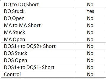
So to
summarize, for this hypothetical example, the boundary-scan test coverage is:
So, the
boundary-scan test coverage for this example is quite poor. Opens coverage is
non-existent, and shorts coverage is very limited. If there is no physical
access for In-Circuit Test (ICT) – which is quite common on today’s designs – how do
we get structural test coverage on memories?
The
solution is to use a combination of other technologies to provide test coverage
which would otherwise be lost. On Intel designs, this would be provided by
processor-controlled test (PCT) and Intel High-Speed I/O (HSIO). For more
information on this, see our eBooks How to Test High-Speed Memory with Non-intrusive Embedded
Instruments or Testing DDR3 Memory with Boundary Scan/JTAG.


