Recent surveys by iNEMI (International Electronics Manufacturing Initiative) validated what many engineers have experienced firsthand. Testing high-speed memories soldered to a circuit board is as elusive as it is critical for overall system performance. Testing DDR3 and DDR4 memory buses can be particularly tricky, given the fact that DDR is so fast and that the bus carries the clock and data on both the rising and falling edges of the signal. Sorting all of that out and making sure it stays sorted out over the life cycle of a system can be a daunting challenge.
By the way, those iNEMI surveys found that engineers are saying that characterizing and testing memory is one of their top three most challenging problems these days.
With memory buses like DDR, the causes of failed memory transfers can go way beyond structural shorts and opens. Clock, data and address signals are vulnerable to temperature, jitter, noise, voltage aberrations, environmental conditions, as well as manufacturing variations in resistance, capacitance, inductance and others. Any or all of these factors can adversely affect the timing of the DDR data window. Often the DDR bus must be tuned by adjusting the parameters of the data window to optimize data throughput. Memory cell faults can cause performance issues and system crashes.
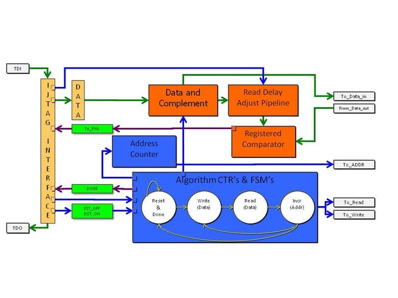
Of course, another complication is the disappearance of access for legacy test equipment that is dependent upon probing the bus. Test pads on circuit boards are vanishing because they devastate the signal integrity on a memory bus. As a result, many engineers are turning to embedded instruments to test memory architectures. Several non-intrusive board test (NBT) methods are available, including boundary-scan, processor-controlled test (PCT), FPGA-controlled test (FCT), functional test and others. Here’s a block diagram of a generic embedded memory test instrument.
Fortunately for engineers, each NBT method has its own set of strengths and advantages which complement effectively the various objectives for memory test during each phase in a product’s life cycle. For example, validating and characterizing the memory architecture on a prototype of a new design during board bring-up involves different constraints and requirements than those encountered when testing a circuit board during volume manufacturing. Likewise, the tools needed by the service organization to support a system in the field require a different set of capabilities. Ultimately, the memory test toolset must be multifaceted so the right tool can be deployed at the right time.
Of course, I’m just scratching the surface on how to test high-speed memory and the many tradeoffs that come with each NBT test method. If you’d like to take a deeper dive, take a look at a new white paper Al Crouch, our chief technologist for core instruments, has just published. It’s 21 pages and chock full of useful information and illustrations.
“How to test high-speed memory with non-intrusive embedded instruments”


