
One of the newest IEEE Standards Committees is currently defining the P1838 3D Test Standard. The main goal of P1838 is to develop a “Per Die” Access Mechanism that becomes a “Stacked Die” Access Mechanism when the individual die are stacked into 3D silicon. The main focus is to handle the configuration of stacking die that are connected to each other using Through-Silicon-Vias (TSV’s) to make 3D silicon integration, which is different from Package-on-Package and other 3D packaging techniques. Find out more…
With 3D packaging, bond wires are still used and there may be access to the individual packaged chips. In addition, the individual chips may be tested in their packages or as bare die with probe pads. However, 3D silicon integration made with TSV’s will most likely not have any access to the interconnects between die, and since the individual die are not made to be packaged separately, they may also not have very many probe pads. TSV’s are extremely large (compared to on-die routes), being of the order of 2 microns (2000 nanometers), and probe pads will be costly, so an economical test and debug access port must be supported (meaning an economy of required test signals on each die and on the completed stack).
BASE die should support 1149.1
Looking at the problem and noting that only the bottom or “BASE” die will have real pins and probe pads (the BASE die is meant to be connected to the board), it's evident that the BASE die will be required to support the 1149.1 JTAG TAP. Even if the BASE die is an interposer or a die without any digital logic, it must still support at least the TCK, TMS, TDI and TDO signals that make up the JTAG TAP. The current thought process, considering that both IC and board test will have to be conducted on the completed stack, is that the 1149.1 TAP and TAP Controller will be the main method by which all of the test and debug logic in the stack will be accessed, configured, controlled, and operated. If the 1149.1 TAP Controller will generate the operation protocol (i.e. the Capture-Shift[n]-Update sequence associated with a ScanDR), then this requires the access mechanism for each die to at least be compatible with JTAG.
In addition, an evaluation of the requirements of each die has resulted in the identification of four basic operations that each die must support in a standalone manner and in a stacked manner. The four operations are:
- A Bypass to skip this Die
- Turn-Around to terminate the scan path at Die
- On-Die Access to access test and debug features contained on this Die
- Next-Die Access to access test and debug features above this die while on-die access is active.
In addition, the Turn-Around feature should be the default operation chosen after an 1149.1 reset function (e.g. passing the 1149.1 Finite-State-Machine [FSM] through Test-Logic-Reset [TLR]) — it will produce the smallest scan path and will manage the case of accessing and operating a broken scan path if one of the Bypass functions on one of the die is broken. Each die can be added to the scan path and verified one die at a time if one of the die in the stack has a broken bypass scan chain.
Using P1687 with P1838 — an elegant solution
P1687, which is the IEEE Standard for the Access of On-Chip Embedded Instruments, can be used to implement a P1838 Access Mechanism. But before we get to describing that, let’s investigate the alternatives. One proposed configuration is to modify IEEE 1500 Core Test wrappers and registers to support new WIR instructions that can be used to select UP instructions and DOWN instructions that represent the 4 functions — there is a lot of overhead involved with this, plus the routing of the SelectWIR signal to a probe pad. Another proposed configuration is to modify an 1149.1 TAP controller to add instructions in a similar manner to the 1500 solution. But including a TAP Controller with an FSM on each die requires some form of FSM synchronization, since die above active die that are in Turn-Around or On-Die Access only should be in TLR while the active die is conducting Capture, Shift, and Update operations, or is parked in Run-Test-Idle (RTI). When an UP instruction is installed into the active die (such as Bypass or Next-Die Access), then the Upper Die’s TAP Controller FSM must enter RTI simultaneous to the Lower Die that is activating the Upper die. And again, to support multiple TAP Controllers in the stack will require that the TMS signal be distributed vertically up through the stack (one more signal, similar to having to add the SelectWIR for the 1500 solution).
Conversely, the P1687 solution would be to gang two Segment-Insertion-Bits (SIB’s) together back-to-back to provide a two-bit embedded instruction register that is self-contained and can open and close scan paths to provide the four functions.
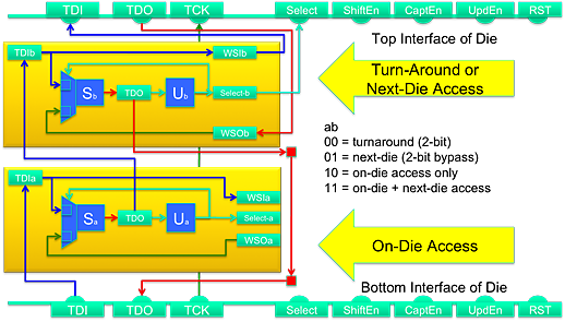
Figure 1: The Two-SIB 3D Interface that Supports the Four Access Functions
As can be seen in Figure 1, the bottom SIB (SIBa) conducts two functions: if there is a logic 0 in the Update Cell (U), then the scan path selected is the path up to the upper SIB (SIBb); if there is a logic 1 in the Update Cell, then the scan path selected is the WSI port that would connect to on-die scan paths and return through the WSO path. The upper SIB (SIBb) also conducts two functions: if there is a logic 0 in its Update Cell, then the scan path selected is the downward path to the TDO port on the bottom die interface; if there is a logic 1 in its Update Cell, then the scan path selected is the upward path to the TDI on the upper die interface and the scan path will return through the TDO on the upper die interface. In aggregate, the two bits provide the truth table shown.
If SIBa|SIBb = 00, then the P1687 Access Unit represents a two-bit Turn-Around function where the scan path will start at the TDI on the bottom die interface, will pass through SIBa, will continue on through SIBb, and will exit downward to the TDO on the bottom die interface.
If SIBa|SIBb = 01, then the 1687 Access Unit represents a two-bit Bypass function where the scan path will start at TDI on the bottom die interface, will pass through SIBa, will bypass SIBb and directly drive the WSI port which connects directly to the TDI at the top die interface — with the return path being through the top die interface TDO that will pass through SIBb and exit through the bottom of die TDO.
If SIBa|SIBb = 10, then the 1687 Access Unit represents the On-Die Access Only function where the scan path will start at the TDI on the bottom die interface, will bypass SIBa and will drive the WSI port directly, which can drive any number of 1500 Wrappers, 1149.1 TDR’s or 1687 SIB’s and TDRs — with the return path being through the WSO that passes through SIBa, then passes through SIBb, and exits through the bottom die interface TDO.
If SIBa|SIBb = 11, then the 1687 Access Unit represent the combined On-Die Access and the Next-Die Access function where the scan path will start at the TDI on the bottom die interface, will bypass SIBa and will drive the WSI port directly, which can drive any number of 1500 Wrappers, 1149.1 TDR’s or 1687 SIB’s and TDRs — with the return path being through through the WSO that passes through SIBa, then travels up to bypass SIBb to drive the SIBb WSI that connects directly to the TDI at the top die interface — with that return path being through the top die interface TDO that will pass through SIBb and exit through the bottom of die TDO.
Note that this SIB has the multiplexor in front of the Shift Cell so that the distribution of TDI become a loading problem instead of the “after the Shift Cell” version of the SIB where the return path may present a long combinational path problem. It is easier for design tools to size buffers and drive strength to manage fanout and loading than it is to manage long combinational paths. Also note that the Select, ShiftEn, CaptureEn, UpdateEn, and Reset signals are shown on both the bottom die and top die interface, but aren’t shown as being routed — this is to prevent clutter in the diagram. The Select Port is passed into a set of AND-gates that enable each of the other SIB operation signals ( ShiftEn, CaptureEn, and UpdateEn), which source from either a tester or from the stack’s TAP Controller — this die can only be operated when “selected” by the tester or the die below, in a similar manner that the Select signal from SIBb will be used to enable the die above this one.
As P1838 moves forward, the Working Group will evaluate the various solutions, will hold them up against the “per die”, “per stack” and other requirements, and will vote on the solutions for them to be included within the Draft Standard. Hopefully, this clean, elegant and minimal implementation solution will be one of the allowed configurations for individual 3D Die that are to be stacked.
One Response
Thanks for very helpful and informative post on P1838 3D Test Standard!