Hello, and welcome—this is the first of a set of short blogs on the topic of 1687. Since 1687 is still in the proposal stage, it is actually referred to as P1687 right now, but the “P” will disappear after the standard is ratified and it is no longer a “proposal”. We are nearing the point where the committee is going to submit the draft of the standard for the ratification process, and there is a lot more interest being generated by early adopters, so there is a need for some explanation, understanding, and analysis concerning the costs, efficiencies, configurations and implementations of 1687 (also referred to as IJTAG, where the “I” means “internal”). This first blog answers the question, “what is IEEE 1687”, and subsequent blogs will cover the topics “who uses IEEE 1687”, “what are the advantages of using IEEE 1687 (why use IEEE 1687)”, and “how to use IEEE 1687.”
One of the problems that became apparent when Core-based chips first hit the market, was that the Design-for-Test (DFT) and Design-for-Debug (DFD) included on or within different cores were made with different selection and access mechanisms. Organizing the chip DFT/DFD from a collection of disparate DFTs/DFDs inside of cores turned out to be a larger and more difficult task than many design organizations anticipated (in some cases, getting the chip DFT/DFD to work became the tall-pole in the design schedule). In addition, many chip design organizations established a practice of using the 1149.1 port and controller as a test/debug controller since it was already going to be there for board test—the package pins were already going to exist, and the 1149.1 controller logic was easily extensible with added instructions and registers for controlling and configuring the test and debug logic.
There were some shortcomings identified in the 1149.1 implementations to include DFT/DFD which led to two main problems: one was creating undue complexity for the 1149.1 board test architecture by adding too many instructions; and the other was that the standard 1149.1 architecture wasn’t flexible enough for the needs of chip design engineers. One of the biggest problems was and still is that the 1149.1 BSDL doesn’t have the capability to adequately describe embedded test and debug instruments and operations. A solution to these two main problems (and many minor problems) was to define a different embedded instrument access architecture and use model than that defined by pure 1149.1 JTAG—and that was the beginning of the IEEE 1687 effort.
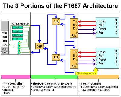
1687 is a proposed IEEE Standard for the access and operation of embedded instruments, and the first iteration of the standard is based on use of the 1149.1 Test Access Port and Controller to provide the chip access—and a set of modified 1149.1-type Test Data Registers (TDRs) to create an access network for embedded instruments. A significant difference over 1149.1 is that the 1687 network allows variable length scan chains—scan chains that can either add or subtract segments or swap between accessible registers during a ScanDR without an intervening ScanIR (or in other words, once the 1687 Instruction is installed into the 1149.1 Instruction Register, the scan chains are configurable and controllable by the data passing through the scan chain as Data Register operations).
The 1687 network architecture allows different configurations to be crafted for embedded instrument access which can be developed to meet various engineering, cost, and operation tradeoffs. These various different architectures can then be described with the Instrument Connectivity Language (ICL) which describes the 1687 TDRs, the scan paths, the variability in scan paths, the connection to the 1149.1 TAP Controller, and the connection between the raw instrument and the 1687 TDR. The true power of the architecture and its description are that they allow instrument vectors, that are written to the instrument interface, to be “retargeted” to the chip’s 1149.1 TAP or even to the board’s/system’s TAP by understanding the description of the access network. This creates an environment for “reuse” of vectors throughout the chip’s lifecycle (cradle-to-grave: meaning—design verification, wafer probe, IC package test, board test, system test, yield-analysis, and customer return test and debug-diagnosis).
The IEEE 1687 Scan Instrument Access Network
These capabilities can provide cost-reduction and work-efficiency to test; can allow the collection of more information for yield-analysis and debug-diagnosis; and allow closer correlation of IC test to board and system test and operation since the same test or instrument can be run in different lifecycle environments. This is the sort of standardized, yet flexible, architecture that is needed to move forward into the future for new technologies such as 3D chips (e.g. Die stacks) and complex hundreds of million gate System-on-a-Chip types of chips.


One Response
Esta es una vista excepcional de la situacin, no creo que bastante he visto desde esa perspectiva antes.
English Translation: “This is an exceptional view of the situation, I do believe, I have not seen enough from that perspective, even considering past experiences.”