
The 2013 Revision of the IEEE 1149.1 Standard incorporates support for dynamic data registers that can change in length and organization, unlike those fixed ones specified by the 2001 Revision. This allows, for example, definition of “excludable segments” for the boundary scan register (BSR); perfect for dealing with BSR segments in different power domains, some powered up and some not. How does this work?
Many ICs today have a need to reduce power consumption. This is especially necessary in the world of mobile and IoT chips, where conserving battery power is an extremely important design consideration. Even high-end devices used in supercomputers are expected to manage their power consumption: for example, the Frontier machine, the USA’s first exascale super, uses up to 20MW, enough to power a small town. Reducing this is important from carbon footprint and total lifecycle cost perspectives.
In ICs, per an example in Ken Parker’s Boundary Scan Handbook Fourth Edition, a floating point unit in a mobile phone may be rarely used, depending on what the user is doing – browsing the web or making a phone call, versus playing a game. In some instances, the FPU may power on and off hundreds of times per second. If this logic block is buried “deep” within the silicon, it won’t affect the BSR. But what if we’re dealing with an I/O logic block such as USB or some GPIO (that may in fact rely on a third-party IP) that has boundary scan register support, with a number of data and control cells, and we want to power that down in a low-power state? At that point, the scan chain is broken, and any test or debug operations are stopped.
How do we prevent the chain from being broken in this example? We divide the chain into segments, each governed by segment-select cell (“SegSel”) that routes traffic around its segment if that domain is not receiving power. A simple illustration of such a segment subject to 1149.1-2013 style control is as below:
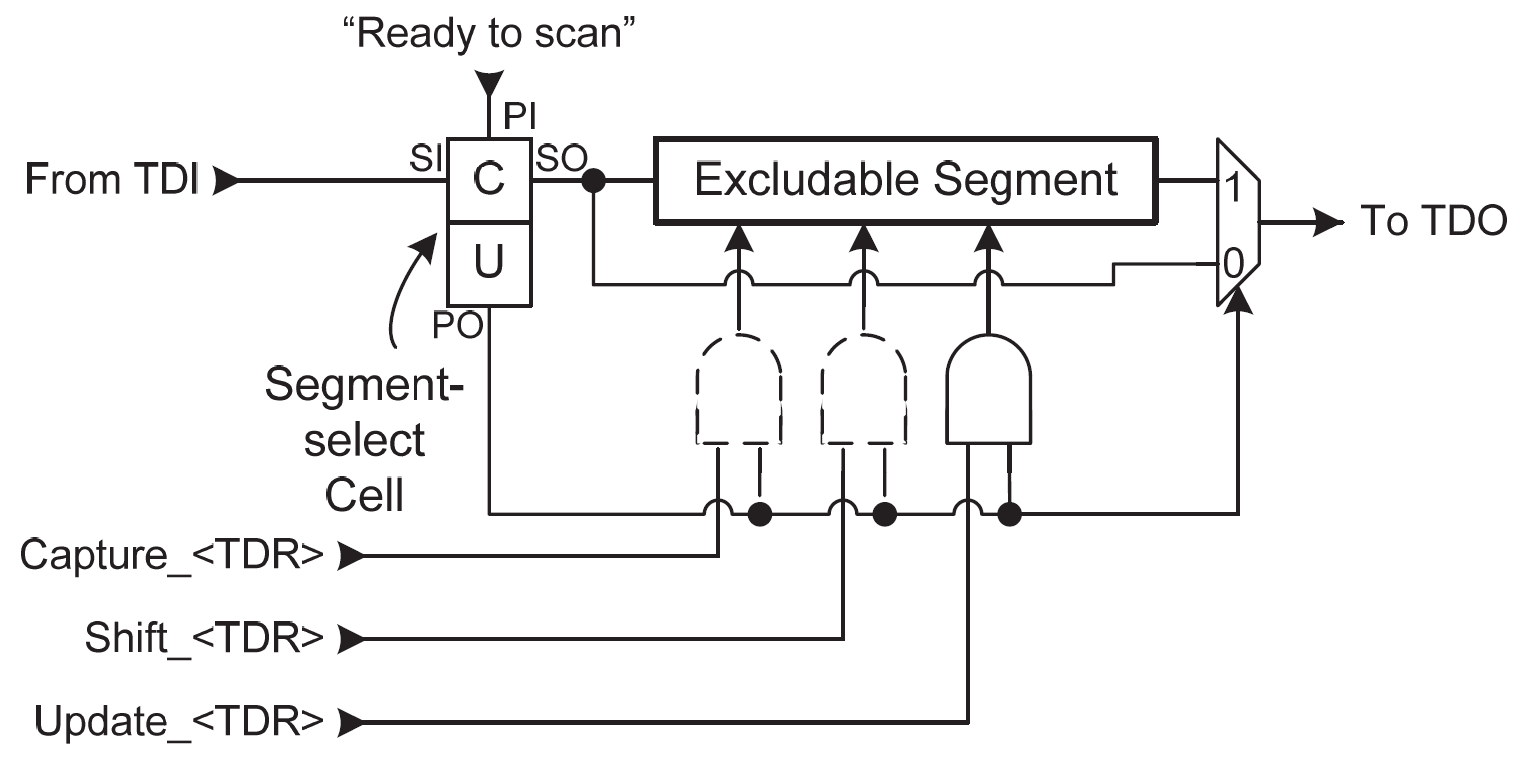
On initial power-on, a device’s boundary scan register will be of minimum length; it then expands and contracts based on the status of power within the associated domains.
A more generalized version of the above is shown with the inclusion of a domain-control cell; this is to take into account that power within a domain can come from on-chip, or it may come from an external source through a power pin. The domain-control cell is used to override an on-chip power controller that may be trying to turn the domain power off. No such control is granted, of course, if the power is coming into the domain externally; but the domain-control cell’s output can be connected to the excludable segment’s external power supply, and request it to supply power, at which point the “Ready to scan” signal is set to “1”:
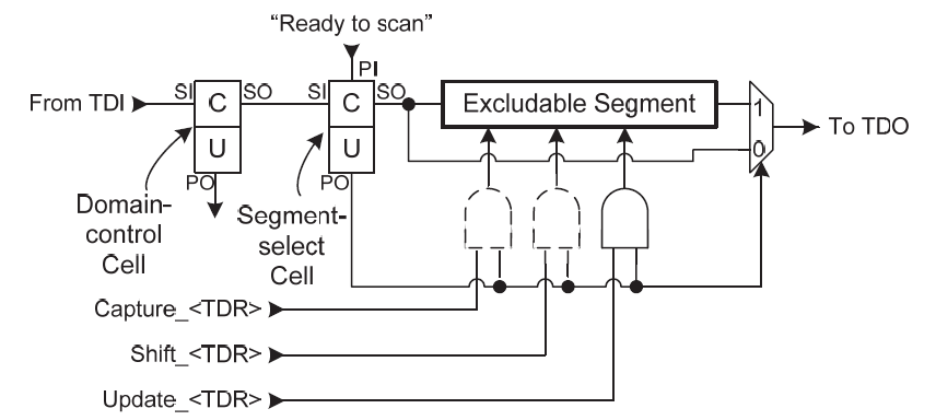
The domain-control cell segment-select cell, and segment select mux (the latter at the far right) are all always powered, and cannot be part of an excludable segment.
Given that this architecture is in place within the IC, how are these excludable segments accounted for within the 2013 BSDL file? Three attributes, ASSEMBLED_BOUNDARY_LENGTH, BOUNDARY_SEGMENT, and REGISTER_ASSEMBLY are used.
Before we show the 2013 example, below is the 2001 BSDL for the venerable TI 74BCT8374 Octal D flip-flop, that has a fixed-sized boundary register, for comparison’s sake:
entity sn74bct8374a is

    generic (PHYSICAL_PIN_MAP : string := "UNDEFINED");

    port (CLK:in bit;

          Q:out bit_vector(1 to 8);

          D:in bit_vector(1 to 8);

          GND, VCC:linkage bit;

          OE_NEG:in bit;

          TDO:out bit;

          TMS, TDI, TCK:in bit;

          NC:linkage bit_vector(1 to 4));

    use STD_1149_1_1990.all; -- Get Standard attributes and definitions

    attribute PIN_MAP of sn74bct8374a : entity is PHYSICAL_PIN_MAP;

    constant JT : PIN_MAP_STRING := "CLK:1, Q:(2,3,4,5,7,8,9, " &

                                    "10), D:(23,22,21,20,19, " &

                                    "17,16,15), GND:6, VCC:18, " &

                                    "OE_NEG:24, TDO:11, TMS:12, " &

                                    "TCK:13, TDI:14";

    constant DW : PIN_MAP_STRING := "CLK:1, Q:(2,3,4,5,7,8,9, " &

                                    "10), D:(23,22,21,20,19, " &

                                    "17,16,15), GND:6, VCC:18,"  &

                                    "OE_NEG:24, TDO:11, TMS:12, " &

                                    "TCK:13, TDI:14";

    constant NT : PIN_MAP_STRING := "CLK:1, Q:(2,3,4,5,7,8,9, " &

                                    "10), D:(23,22,21,20,19, " &

                                    "17,16,15), GND:6, VCC:18, " &

                                    "OE_NEG:24, TDO:11, TMS:12, " &

                                    "TCK:13, TDI:14";

    constant FK : PIN_MAP_STRING := "CLK:9, Q:(10,11,12,13,16,17," &

                                    "18,19), D:(6,5,4,3,2,27,26,25), " &

                                    "GND:14, VCC:28, OE_NEG:7, " &

                                    "TDO:20, TMS:21, TCK:23, TDI:24," &

                                    "NC:(1,8,15,22)";

    attribute TAP_SCAN_IN    of TDI : signal is true;

    attribute TAP_SCAN_MODE  of TMS : signal is true;

    attribute TAP_SCAN_OUT   of TDO : signal is true;

    attribute TAP_SCAN_CLOCK of TCK : signal is (20.0e6, BOTH);

    attribute INSTRUCTION_LENGTH of sn74bct8374a : entity is 8;

    attribute INSTRUCTION_OPCODE of sn74bct8374a : entity is

            "BYPASS (11111111, 10001000, 00000101, 10000100, 00000001), " &

            "EXTEST (00000000, 10000000),"  &

            "SAMPLE (00000010, 10000010),"  &

            "INTEST (00000011, 10000011),"  &

            "HIGHZ  (00000110, 10000110),"  & -- Bypass with outputs high-z

            "CLAMP  (00000111, 10000111),"  & -- Bypass with bs values

            "RUNT   (00001001, 10001001),"  & -- Boundary run test

            "READBN (00001010, 10001010),"  & -- Boundary read normal mode

            "READBT (00001011, 10001011),"  & -- Boundary read test mode

            "CELLTST(00001100, 10001100),"  & -- Boundary selftest normal

            "TOPHIP (00001101, 10001101),"  & -- Boundary toggle out test

            "SCANCN (00001110, 10001110),"  & -- BCR scan normal

            "SCANCT (00001111, 10001111)"   ; -- BCR scan test

    attribute INSTRUCTION_CAPTURE of sn74bct8374a : entity is "10000001";

    attribute INSTRUCTION_DISABLE of sn74bct8374a : entity is "HIGHZ";

    attribute INSTRUCTION_GUARD   of sn74bct8374a : entity is "CLAMP";

    attribute REGISTER_ACCESS of sn74bct8374a : entity is

            "BOUNDARY (EXTEST, SAMPLE, INTEST, READBN, READBT, CELLTST)," &

            "BYPASS   (BYPASS, HIGHZ, CLAMP, RUNT, TOPHIP)," &

            "BCR[2]   (SCANCN, SCANCT)" ;

    attribute BOUNDARY_CELLS    of sn74bct8374a : entity is "BC_1";

    attribute BOUNDARY_LENGTH   of sn74bct8374a : entity is 18;

    attribute BOUNDARY_REGISTER of sn74bct8374a : entity is

    " 0 (BC_1, Q(8)  ,output3, X, 16, 1, Z), "  &

    " 1 (BC_1, Q(7)  ,output3, X, 16, 1, Z), "  &

    " 2 (BC_1, Q(6)  ,output3, X, 16, 1, Z), "  &

    " 3 (BC_1, Q(5)  ,output3, X, 16, 1, Z), "  &

    " 4 (BC_1, Q(4)  ,output3, X, 16, 1, Z), "  &

    " 5 (BC_1, Q(3)  ,output3, X, 16, 1, Z), "  &

    " 6 (BC_1, Q(2)  ,output3, X, 16, 1, Z), "  &

    " 7 (BC_1, Q(1)  ,output3, X, 16, 1, Z), "  &

    " 8 (BC_1, D(8)  ,input  , X), " &

    " 9 (BC_1, D(7)  ,input  , X), " &

    "10 (BC_1, D(6)  ,input  , X), " &

    "11 (BC_1, D(5)  ,input  , X), " &

    "12 (BC_1, D(4)  ,input  , X), " &

    "13 (BC_1, D(3)  ,input  , X), " &

    "14 (BC_1, D(2)  ,input  , X), " &

    "15 (BC_1, D(1)  ,input  , X), " &

    "16 (BC_1, OE_NEG,input  , X), " & -- merged Input/Control cell

    "16 (BC_1, *     ,control, 1), " & -- merged input/control cell

    "17 (BC_1, CLK   ,input  , X)  " ;

end sn74bct8374a;
Note that the 74BCT8374 device has a fixed boundary register, with BOUNDARY_LENGTH having a value of 18, and the BOUNDARY_REGISTER as described above.
In a device with excludable BSR segments that conforms to IEEE 1149.1-2013, BOUNDARY_LENGTH is replaced by ASSEMBLED_BOUNDARY_LENGTH, and BOUNDARY_REGISTER is replaced by BOUNDARY_SEGMENT. Further, REGISTER_ASSEMBLY stitches the BSR together, effectively “flattening” it based on the included/excluded status of chains within power domains.
Let’s look at what this looks like for a hypothetical device named “Chip2013”. We’ll create the first two attributes as follows:
Attribute ASSEMBLED_BOUNDARY_LENGTH of Chip2013 : entity

     is (17, 22); -- Minimum length 17, Maximum length 22

Attribute BOUNDARY_SEGMENT of Chip2013 : entity is

     “North [5] (“&

     -- num cell port function safe [ccell disval rslt]

          “4 (BC_1, *, controlr, 1 ), “&

          “3 (BC_1, N_D(1), input, X, PULL0), “&

          “2 (BC_1, N_D(0), input, X, PULL0), “&

          “1 (BC_1, N_Q(1), output3, X, 10, 4, PULL0), “&

          “0 (BC_1, N_Q(0), output3, X, 10, 4, PULL0)), “&

     “South [5] (“&

     -- num cell port function safe [ccell disval rslt]

          “4 (BC_1, *, controlr, 1 ), “&

          “3 (BC_1, S_D(1), input, X, PULL0), “&

          “2 (BC_1, S_D(0), input, X, PULL0), “&

          “1 (BC_1, S_Q(1), output3, X, 10, 4, PULL0), “&

          “0 (BC_1, S_Q(0), output3, X, 10, 4, PULL0)), “&

     “West [5] (“&

     -- num cell port function safe [ccell disval rslt]

          “4 (BC_1, *, controlr, 1 ), “&

          “3 (BC_1, W_D(1), input, X, PULL0), “&

          “2 (BC_1, W_D(0), input, X, PULL0), “&

          “1 (BC_1, W_Q(1), output3, X, 10, 4, PULL0), “&

          “0 (BC_1, W_Q(0), output3, X, 10, 4, PULL0)), “&

     “East [5] (“&

     -- num cell port function safe [ccell disval rslt]

          “4 (BC_1, *, controlr, 1 ), “&

          “3 (BC_1, E_D(1), input, X, PULL0), “&

          “2 (BC_1, E_D(0), input, X, PULL0), “&

          “1 (BC_1, E_Q(1), output3, X, 10, 4, PULL0), “&

          “0 (BC_1, E_Q(0), output3, X, 10, 4, PULL0)), “;
The rest of this example will make sense once we also display the REGISTER_ASSEMBLY attribute:
Attribute REGISTER_ASSEMBLY of Chip2013 : entity IS

     “Boundary ( “&        -- This instantiates the BSR

     “(North IS North), “& -- This identifies the first segment

     “(South IS South), “& -- This identifies the 2nd segment

     -- The next three lines describe a domain control cell

     -- and segment selection cell

     “(PowerUp IS DomCtrl Domain(PwrEast) TAPReset), “&

     “(East_Start IS SegSel Domain(PwrEast) “&

           “Segment(SegEast) TAPReset), “&

     “(East IS East), “&   -- The excludable East segment

     -- The next line shows the zero-length segment mux

     “(East_End IS SegMux Segment(SegEast)), “&

     “(West IS West) )”;   -- Fourth segment
In this excerpt from the BSDL, the domain control cell is named PowerUp, and it controls the PwrEast power domain. At power-on, the PowerUp domain control cell is reset by TAPReset, so the PwrEast domain won’t have power then.
Also, the associated segment control cell is named East_Start, which includes or excludes the SegEast segment that resides in the PwrEast power domain. Like the PowerUp domain control cell, the East_Start segment control cell is reset by TAPReset, so at power-on the SegEast segment is excluded.
Now that we have all three attributes listed, we can see what the boundary scan register looks like with the East segment excluded:
-- num cell port function safe [ccell disval rslt]

     “16(BC_1, *, controlr, 1), “&

     “15(BC_1, N_D(1), input, X, PULL0), “&

     “14(BC_1, N_D(0), input, X, PULL0), “&

     “13(BC_1, N_Q(1), output3, X, 16, 1, PULL0), “&

     “12(BC_1, N_Q(0), output3, X, 16, 1, PULL0), “&

     “11(BC_1, *, controlr, 1), “&

     “10(BC_1, S_D(1), input, X, PULL0), “&

     “9 (BC_1, S_D(0), input, X, PUL0), “&

     “8 (BC_1, S_Q(1), output3, X, 11, 1, PULL0), “&

     “7 (BC_1, S_Q(0), output3, X, 11, 1, PULL0), “&

     “6 (PowerUp), “&

     “5 (East_Start), “&

     “4 (BC_1, *, controlr, 1), “&

     “3 (BC_1, W_D(1), input, X, PULL0), “&

     “2 (BC_1, W_D(0), input, X, PULL0), “&

     “1 (BC_1, W_Q(1), output3, X, 4, 1, PULL0), “&

     “0 (BC_1, W_Q(0), output3, X, 4, 1, PULL0), “;
Note that cells 6 and 5 are the domain and control cells, respectively; and that they appear between the West and South segments. The REGISTER_ASSEMBLY attribute lists the segment closest to TDI (North) first and the segment driving TDO (West) last; and hence the above lists segments North, South and West respectively, with East excluded. Including the two cells for domain control and segment selection are included, the total assembled boundary scan register length is 1 + 1 + 5 + 5 + 5 = 17; exactly what is called out for the minimum ASSEMBLED_BOUNDARY_LENGTH.
Now let’s assume that the East segment is included, and just stitch everything together:
-- num cell port function safe [ccell disval rslt]

     “21(BC_1, *, controlr, 1), “&

     “20(BC_1, N_D(1), input, X, PULL0), “&

     “19(BC_1, N_D(0), input, X, PULL0), “&

     “18(BC_1, N_Q(1), output3, X, 21, 1, PULL0), “&

     “17(BC_1, N_Q(0), output3, X, 21, 1, PULL0), “&

     “16(BC_1, *, controlr, 1), “&

     “15(BC_1, S_D(1), input, X, PULL0), “&

     “14(BC_1, S_D(0), input, X, PUL0), “&

     “13(BC_1, S_Q(1), output3, X, 16, 1, PULL0), “&

     “12(BC_1, S_Q(0), output3, X, 16, 1, PULL0), “&

     “11(PowerUp), “&

     “10(East_Start), “&

     “9 (BC_1, *, controlr, 1), “&

     “8 (BC_1, E_D(1), input, X, PULL0), “&

     “7 (BC_1, E_D(0), input, X, PULL0), “&

     “6 (BC_1, E_Q(1), output3, X, 9, 1, PULL0), “&

     “5 (BC_1, E_Q(0), output3, X, 9, 1, PULL0), “&

     “4 (BC_1, *, controlr, 1), “&

     “3 (BC_1, W_D(1), input, X, PULL0), “&

     “2 (BC_1, W_D(0), input, X, PULL0), “&

     “1 (BC_1, W_Q(1), output3, X, 4, 1, PULL0), “&

     “0 (BC_1, W_Q(0), output3, X, 4, 1, PULL0) “;
You can see now that the total number of cells is 22, which is the maximum ASSEMBLED_BOUNDARY_LENGTH of Chip2013.
Whew! Did that seem complicated? It certainly seemed that way when I started looking at it, but after some study, it became much clearer. Of course, in this exercise I “manually” constructed the BSR based on eyeballing the BOUNDARY_SEGMENT and REGISTER_ASSEMBLY definitions, and then generated “flattened” output BSDLs that exclude and then include the East power domain. This was for illustrative and educational purposes only; in real life, a boundary scan tool (such as is available with our ScanWorks product) would use software to parse the 2013-compliant BSDL and automatically generate a UUT model for the design with far less opportunity for error.
If you’d like to learn more about boundary scan in general, I’d highly recommend an article just written by ASSET’s Michael Johnson, Everything You Need to Know about ScanWorks Interconnect (Part 3). It’s the third of a multi-part series on the topic of JTAG; very well-suited for engineers with beginner to intermediate level knowledge of boundary scan. For more detail, you can always look at our JTAG and Boundary Scan Tutorial, Second Edition eBook. And if you really want to go even deeper and can afford it, I can recommend Ken Parker’s Boundary Scan Handbook, 4th Edition (from which the above excludable segment example was derived; available via Amazon and other online book sellers), or the IEEE 1149.1-2013 specification itself, available from www.techstreet.com.