In the last blog, I explored the JTAG scan path of the ScanLite demonstration board. In this article, I do a deeper dive into what options are available within ScanWorks to verify the scan path, and explore some of the underlying technology of IEEE 1149.1.
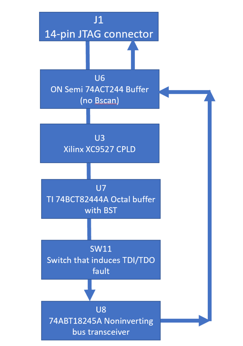
I thought at this point that it would be useful to draw up a functional block diagram of the ScanLite’s scan chain:
ScanWorks contains what it calls an “Action” named Scan Path Verify that performs the following functions:
- Checks the integrity of the scan path and UUT interface
- Verifies the scan path length
- Verifies the correct order of the devices in the scan path
- Helps validate the design description
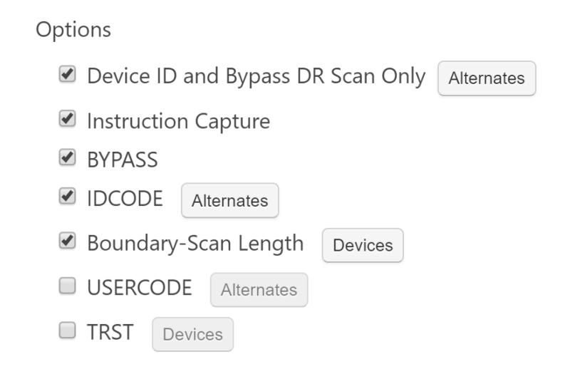
The scan path is the very first thing to check, before running any of the other actions. And we saw from last time that there are numerous options to test and tweak the scan path, in case it is giving trouble:
Diving into each of these in some more detail, I see the following descriptions from the ScanWorks Help:
Device ID and Bypass DR Scan Only: Tests all components in the scan path by using default Device ID or BYPASS instructions.
Instruction Capture: Checks the instruction register capture value for all devices in the scan path.
BYPASS: Checks the scan path with all devices in BYPASS.
IDCODE: Verifies that the actual ID codes match those defined in the BSDL (boundary scan description language) file. It does this by scanning in the IDCODE instruction.
Boundary-Scan Length: Puts each device into SAMPLE, with all other devices in BYPASS. Then DR scans are done with patterns of 0s and 1s during overshifting.
USERCODE: Verifies that the actual user codes match those defined in the BSDL.
TRST: Test the function of the TRST signal in user-specified devices, one at a time.
There are a lot of new terms here. To understand this better, we’re going to need to take a short detour into the technology behind JTAG and boundary scan.
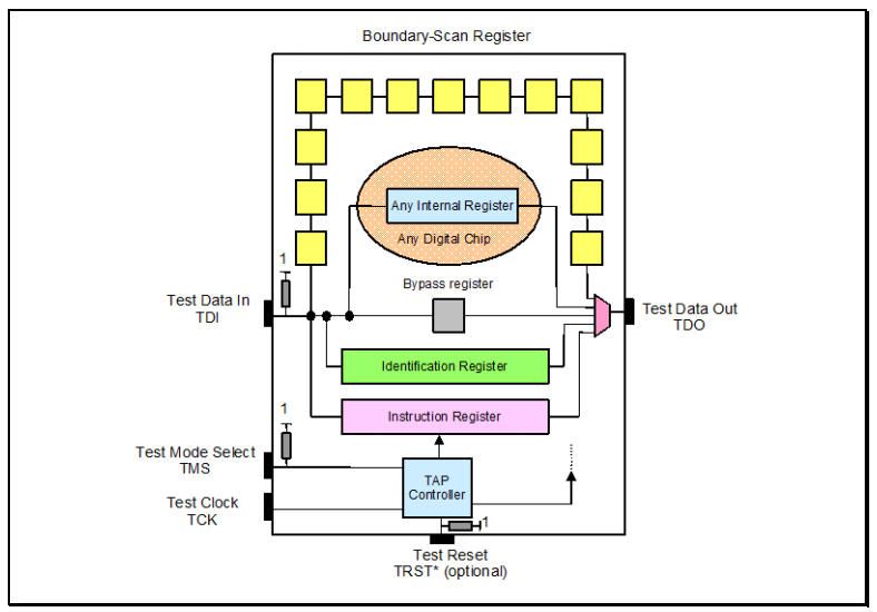
Boundary scan is a technology whose foundation rests upon the JTAG architecture specified in IEEE 1149.1, that was standardized in 1990. Boundary scan is now mostly synonymous with JTAG, but JTAG has essential uses (such as debug, and device programming) beyond simply manufacturing test applications. The overall architecture of JTAG within a chip is as per the below:
The architecture has the following main components:
Four dedicated test pins — Test Data In (TDI), Test Mode Select (TMS), Test Clock (TCK), Test Data Out (TDO) — and one optional test pin Test Reset (TRST*). These pins are collectively referred to as the Test Access Port (TAP).
Boundary-scan cells (in yellow) on the device primary input and primary output pins, connected internally to form a serial boundary-scan register (Boundary Scan Register).
A finite-state machine TAP controller with inputs TCK, TMS, and TRST* (the block in light blue)
An n-bit (n ≥ 2) Instruction Register (IR), holding the current instruction (the purple block).
A 1-bit BYPASS register (gray block).
An optional 32-bit Identification Register capable of being loaded with a permanent device identification code (the green block).
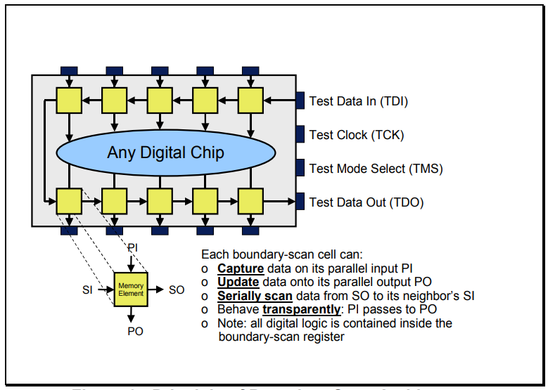
Before we continue, it’s worthwhile taking a closer look at the blocks in yellow, the boundary-scan cells. We can see below that they are essentially memory elements, that in normal mode just pass data transparently to/from the chip’s core logic:
On a chip, each primary input signal and primary output signal is supplemented with a multi-purpose memory element called a boundary-scan cell (in yellow above). The collection of boundary-scan cells is configured into an extended parallel-in, parallel-out shift register. A parallel load operation, called a “capture” operation, causes signal values on device input pins to be loaded into input cells, and signal values passing from the core logic to device output pins to be loaded into output cells. A parallel unload operation, called an “update” operation, causes signal values already present in the output scan cells to be passed out through the device output pins; and depending on the nature of the input scan cells, signal values already present in the input scan cells will be passed into the core logic.
Data can also be shifted around the shift register in serial mode, starting from a dedicated device input pin called “Test Data In” (TDI) and terminating at a dedicated device output pin called “Test Data Out” (TDO). The test clock, TCK, is fed in via yet another dedicated device input pin and the mode of operation is controlled by a dedicated “Test Mode Select” (TMS) serial control signal.
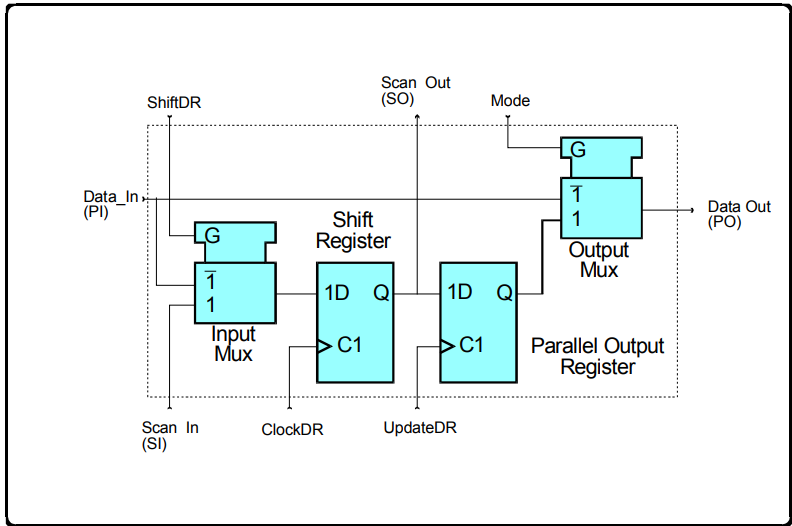
OK, that was a lot to digest. But, one more thing. The circuitry of a basic boundary scan cell is below:
You can see the PI, PO, SI and SO signals as from the prior diagram. During normal mode, Data_In is passed straight through to Data_Out. During update mode, the content of the output register is passed through to Data_Out. During capture mode, the Data_In signal is routed to the shift register and the value is captured by the next ClockDR. During shift mode, the Scan_Out of one register flip-flop is passed to the Scan_In of the next via a hard-wired path. Note that both capture and shift operations do not interfere with the normal passing of data from the PI terminal to the PO terminal – which is really the key power of JTAG.
Well, that’s enough for today. Next week, we’ll see how this all fits together, by running the Scan Path Verify action on the ScanLite board, and then inserting faults and seeing what happens.
Want more detail on JTAG and boundary scan than what you can read here or in Wikipedia? I’d recommend our Boundary Scan Tutorial (note: requires registration).


