Ever since the very beginning of the electronics industry, the finger pointing has been nonstop. Malfunctions in a system or a circuit board as it rolls off the assembly line have to be diagnosed, of course. When they are, the chip supplier likely attributes the cause to the board. But the board manufacturer probably points to a chip as the culprit. And so the finger pointing begins.
Part of the problem over the years has been that chip designers and manufacturing engineers perform their own set of tests to characterize and verify device-level performance while system or board design and manufacturing engineers use another completely distinct set of tests. There’s been no commonality between the two that might reveal, for example, that the chip behaved differently in isolation than it did in a system. Or, that in the system, the chip is still behaving the same way it did when it was designed and manufactured. This kind of information would help pinpoint whether the cause of a problem in the system was in a chip or the circuit board.
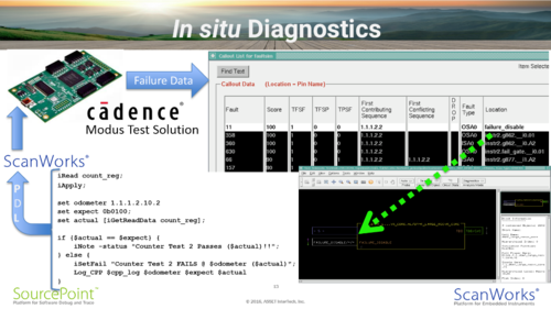
Fortunately, this situation is changing. Next week in Santa Clara at the CDNLive Cadence users group conference, ASSET and Cadence will demonstrate and discuss in situ chip  diagnostics. Essentially, we will show how tests generated by instrumentation embedded in chips can not only characterize and diagnose a chip in isolation before it has been assembled on a circuit board, but also how those same tests using the same embedded instruments can be reapplied in situ, or in the system after the chip has been soldered down on a circuit board.
There are several enablers to achieving in situ diagnostics. One is the interoperability between Cadence’s Modus Test Solution and ASSET’s ScanWorks platform. A second enabler is the IEEE 1687 Internal JTAG (IJTAG) standard. IJTAG provides the functionality that makes interoperability between EDA tools and system circuit board test tools possible.
You may be wondering: “why is this interoperability important? We haven’t had it before and the industry has done all right.” The fact of the matter is, we – providers of tools for chip and board suppliers – could do better by each other and for the end user, who ultimately drives the industry.
Frankly, not all chips and circuit boards are perfect. During the chip design process, the system environment is simulated and a chip is tested and characterized in the abstract world of simulation. Unfortunately, stuff happens in the real world. Manufacturing processes drift out of range, devices and boards end up with variances, and unwanted faults and failures occur. Now, without end-to-end chip-to-system interoperability, diagnosing problems on a circuit board often means that a chip has to be physically removed from the board and returned to the chip vendor for analysis. A slow, expensive and labor-intensive process that often damages the chip or the circuit board. In addition, the removal of the chip from the board may actually impede failure diagnosis since the removal isolates any chip failures from the original environment where the failures were observed. With end-to-end tool interoperability enabled by IJTAG, chips can be diagnosed in situ.
If you’re in Santa Clara next week and will be attending CDNLive, you’ll be able to see a demonstration of the process. For those who won’t make it, I’ve included one of the slides from our presentation that shows how it works.
Here is the link for registering to the CDNLive event: ASSET will be presenting with Cadence on Tuesday (April 5, 2016). Here are the details:
Session Name: Improving Diagnostics from Silicon to System using IEEE 1687 (IJTAG)
Track: Front-end Design
Session #: FED105
Date: 4/5/2016
Time: 4:40PM-5:20PM
And if I’ve piqued your interest in IJTAG, you can download a free tutorial on the standard from our eResources center. Click here.


