In recent years, the increasing size of flash memory has driven device programming to offline methods. However, new techniques are significantly reducing in-system programming times, making it much more feasible and convenient to program flash memory after it’s already been soldered to the board.
In-system programming of flash memory occurs when the flash device is already soldered on the board. Offline programming is done before the device is put down on the PCB. Although batch offline programming is quick and convenient, there are many cases where it is necessary to do programming in-system:
- The flash image needs updating after the board is assembled
- Removing the flash device from the PCB could damage it
- Configure-to-order involves updating flash memory
- One production step involves both test and programming.
For all of the above, programming of memories in-system increases the designer’s and the manufacturing engineer’s flexibility and increases the efficiency of the entire design and engineering process.
Normally, in-system programming involves some sort of JTAG access, where for example a SPI flash device is subtending from an FPGA. Most memory devices don’t directly support JTAG access, but they can be indirectly programmed by way of the FPGA's boundary-scan TAP.
The three main mechanisms for programming such a configuration are via the Boundary-Scan Chain Access method, the Shortened Boundary-Scan Chain method, and SPI Master IP with FIFO Memory method.
Boundary-Scan Chain Access
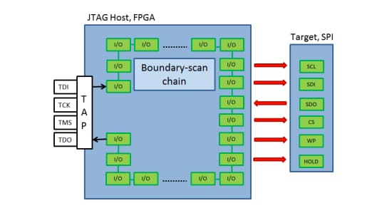
In this method, the data to be programmed is simply routed through the FPGA’s internal boundary scan chain and output to the targeted SPI memory device: 
This technique is the easiest, but also the slowest. All the boundary scan cells (of which there can be thousands in a large FPGA) must be traversed to perform the programming.
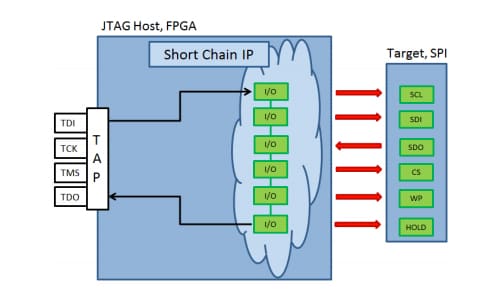
Shortened Boundary-Scan Chain
This involves writing some code to shorten the boundary-scan register chain from say 3,000 cells down to 10-20, so it is much faster: 
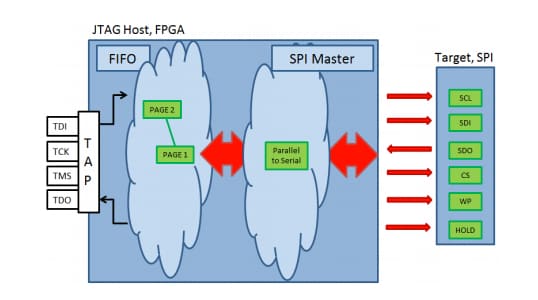
SPI Master IP with FIFO Memory
The most sophisticated method of the three, this uses special logic including a SPI Master and page optimization IP programmed into the FPGA. Programming data is streamed through an IJTAG network into FIFO memory within the FPGA that matches the page size of the SPI memory device (note that IJTAG is used because of the flexibility of having different test and logic blocks simultaneously instantiated within the FPGA). In parallel, the SPI Master is programming the data into the targeted device. Well-designed IP can achieve the maximum programming speed of the SPI device: 
The speeds of the three methods were measured on an Opal Kelly demo board, hosting a Xilinx Spartan 6 FPGA with an attached 2MB SPI device:
|
Method |
Erase/Program/Verify Time |
|
Boundary-Scan Chain Access |
4,620 seconds (77 minutes) |
|
Shortened Boundary-Scan Chain |
465 seconds (7 mins, 45 secs) |
|
SPI Master IP with FIFO Memory |
38 seconds |
For more information on the technology behind these methods, see our eBook, At-Speed SPI Flash/ EEPROM Programming using FPGA and JTAG. Note: requires registration.


